Altera Corporation 1–33
July 2005 Stratix Device Handbook, Volume 2
General-Purpose PLLs in Stratix & Stratix GX Devices
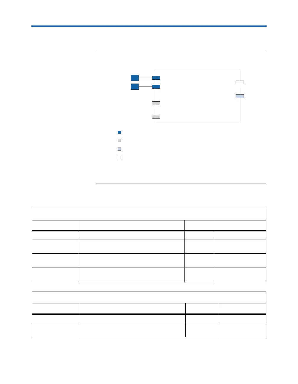
Figure 1–18 shows all possible ports related to fast PLLs.
Figure 1–18. Fast PLL Ports & Physical Destinations
Notes to Figure 1–18:
(1) This input pin is shared by all enhanced and fast PLLs.
(2) This input pin is either single-ended or differential.
Tables 1–10 and 1–11 show the description of all fast PLL ports.
clk[2..0]
locked
pllena
inclk0
areset
pfdena
Fast PLL Signals
(1)
(2)
Physical Pin
Signal Driven by Internal Logic
Signal Driven to Internal Logic
Internal Clock Signal
Table 1–10. Fast PLL Input Signals
Name Description Source Destination
inclk1
Reference clock input to PLL Pin PFD
pllena
Enable pin for enabling or disabling all or a set of
PLLs – active high
Pin PLL control signal
areset
Signal used to reset the PLL which re-
synchronizes all the counter outputs⎯active high
Logic array PLL control signal
pfdena
Enables the up/down outputs from the phase-
frequency detector⎯active high
Logic array PFD
Table 1–11. Fast PLL Output Signals
Name Description Source Destination
clk[2..0]
PLL outputs driving regional or global clock PLL counter Internal clock
locked
Lock output from lock detect circuit⎯active high PLL lock
detect
Logic array