UM10462 All information provided in this document is subject to legal disclaimers. © NXP B.V. 2016. All rights reserved.
User manual Rev. 5.5 — 21 December 2016 11 of 523
NXP Semiconductors
UM10462
Chapter 1: LPC11U3x/2x/1x Introductory information
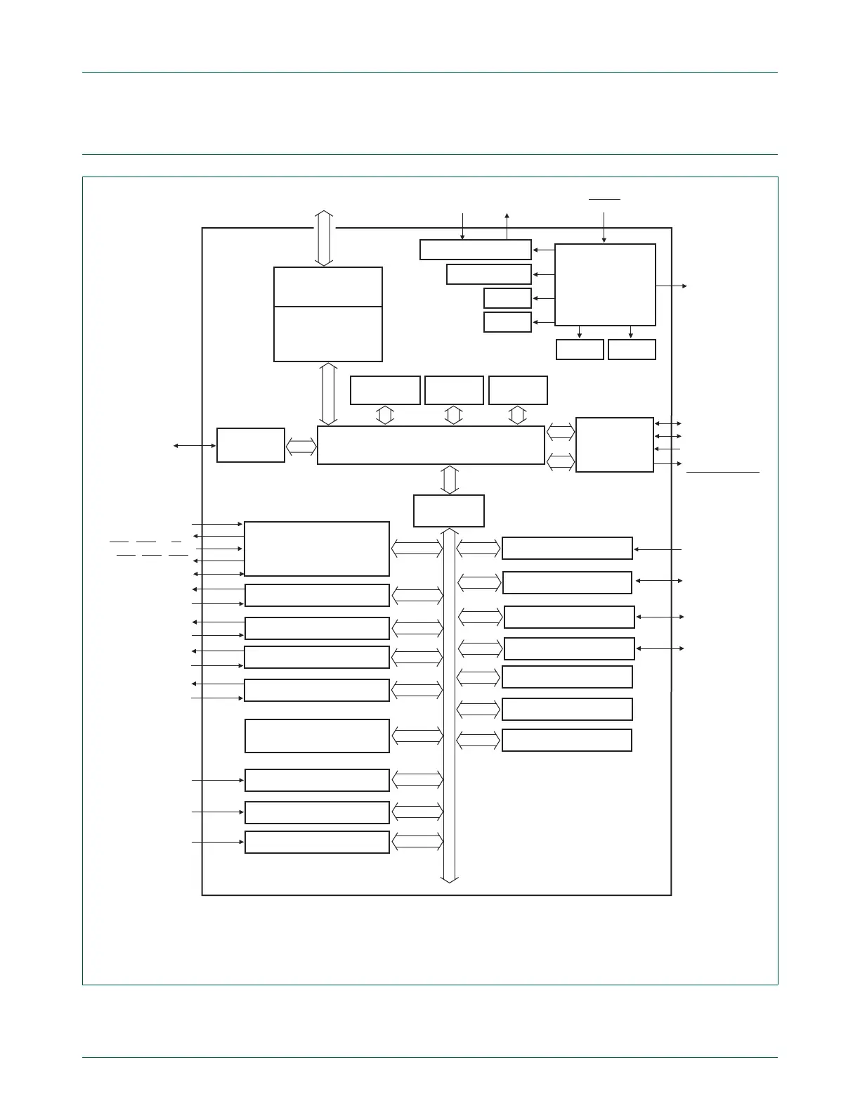
1.4 Block diagram
(1) Function not available on the HVQFN33 package.
(2) CT32B1_CAP1 is only available on the TFBGA48 package.
Fig 1. Block diagram (LPC11U1x)
SRAM
6 kB
ARM
CORTEX-M0
TEST/DEBUG
INTERFACE
FLASH
16/24/32 kB
HIGH-SPEED
GPIO
AHB TO APB
BRIDGE
CLOCK
GENERATION,
POWER CONTROL,
SYSTEM
FUNCTIONS
RESET
SWD, JTAG
LPC11U12/13/14
slave
slave
slave slave
ROM
16 kB
slave
AHB-LITE BUS
GPIO ports 0/1
CLKOUT
IRC, WDO
SYSTEM OSCILLATOR
POR
PLL0 USB PLL
BOD
10-bit ADC
USART/
SMARTCARD INTERFACE
AD[7:0]
RXD
TXD
CTS, RTS, DTR
SCLK
GPIO PIN INTERRUPTS
32-bit COUNTER/TIMER 0
CT32B0_MAT[3:0]
CT32B0_CAP[1:0]
(1)
32-bit COUNTER/TIMER 1
CT32B1_MAT[3:0]
CT32B1_CAP[1:0]
(2)
DCD, DSR
(1)
, RI
(1)
16-bit COUNTER/TIMER 1
WINDOWED WATCHDOG
TIMER
GPIO GROUP0 INTERRUPT
CT16B1_MAT[1:0]
16-bit COUNTER/TIMER 0
CT16B0_MAT[2:0]
CT16B0_CAP0
CT16B1_CAP0
GPIO pins
GPIO pins
GPIO GROUP1 INTERRUPT
GPIO pins
system bus
SSP0
SCK0, SSEL0,
MISO0, MOSI0
SSP1
SCK1, SSEL1,
MISO1, MOSI1
I
2
C-BUS
IOCON
SYSTEM CONTROL
PMU
SCL, SDA
XTALIN XTALOUT
USB DEVICE
CONTROLLER
USB_DP
USB_DM
USB_VBUS
USB_FTOGGLE,
USB_CONNECT
002aaf885
master
slave

 Loading...


