UM10462 All information provided in this document is subject to legal disclaimers. © NXP B.V. 2016. All rights reserved.
User manual Rev. 5.5 — 21 December 2016 84 of 523
NXP Semiconductors
UM10462
Chapter 7: LPC11U3x/2x/1x I/O configuration
7.4 Register description
The I/O configuration registers control the PIO port pins, the inputs and outputs of all
peripherals and functional blocks, the I
2
C-bus pins, and the ADC input pins.
Each port pin PIOn_m has one IOCON register assigned to control the pin’s function and
electrical characteristics.
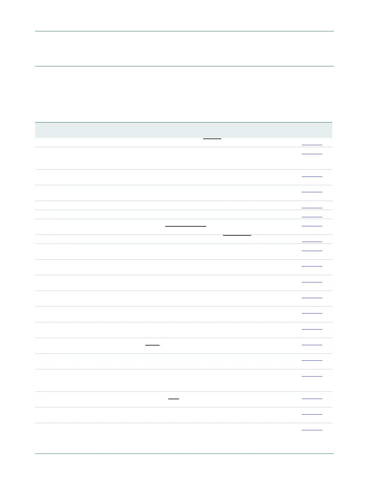
Table 75. Register overview: I/O configuration (base address 0x4004 4000)
Name Access Address
offset
Description Reset value Reference
RESET_PIO0_0 R/W 0x000 I/O configuration for pin RESET
/PIO0_0 0x0000 0090 Table 76
PIO0_1 R/W 0x004 I/O configuration for pin
PIO0_1/CLKOUT/CT32B0_MAT2/USB_FTO
GGLE
0x0000 0090 Table 77
PIO0_2 R/W 0x008 I/O configuration for pin
PIO0_2/SSEL0/CT16B0_CAP0/IOH_0
0x0000 0090 Table 78
PIO0_3 R/W 0x00C I/O configuration for pin
PIO0_3/USB_VBUS/IOH_1
0x0000 0090 Table 79
PIO0_4 R/W 0x010 I/O configuration for pin PIO0_4/SCL/IOH_2 0x0000 0080 Table 80
PIO0_5 R/W 0x014 I/O configuration for pin PIO0_5/SDA/IOH_3 0x0000 0080 Table 81
PIO0_6 R/W 0x018 I/O configuration for pin
PIO0_6/USB_CONNECT
/SCK0/IOH_4
0x0000 0090 Table 82
PIO0_7 R/W 0x01C I/O configuration for pin PIO0_7/CTS/IOH_5 0x0000 0090 Table 83
PIO0_8 R/W 0x020 I/O configuration for pin
PIO0_8/MISO0/CT16B0_MAT0/R/IOH_6
0x0000 0090 Table 84
PIO0_9 R/W 0x024 I/O configuration for pin
PIO0_9/MOSI0/CT16B0_MAT1/R/IOH_7
0x0000 0090 Table 85
SWCLK_PIO0_10 R/W 0x028 I/O configuration for pin SWCLK/PIO0_10/
SCK0/CT16B0_MAT2
0x0000 0090 Table 86
TDI_PIO0_11 R/W 0x02C I/O configuration for pin
TDI/PIO0_11/AD0/CT32B0_MAT3
0x0000 0090 Table 87
TMS_PIO0_12 R/W 0x030 I/O configuration for pin
TMS/PIO0_12/AD1/CT32B1_CAP0
0x0000 0090 Table 88
TDO_PIO0_13 R/W 0x034 I/O configuration for pin
TDO/PIO0_13/AD2/CT32B1_MAT0
0x0000 0090 Table 89
TRST_PIO0_14 R/W 0x038 I/O configuration for pin
TRST
/PIO0_14/AD3/CT32B1_MAT1
0x0000 0090 Table 90
SWDIO_PIO0_15 R/W 0x03C I/O configuration for pin
SWDIO/PIO0_15/AD4/CT32B1_MAT2
0x0000 0090 Table 91
PIO0_16 R/W 0x040 I/O configuration for pin
PIO0_16/AD5/CT32B1_MAT3/IOH_8
WAKEUP
0x0000 0090 Table 92
PIO0_17 R/W 0x044 I/O configuration for pin
PIO0_17/RTS
/CT32B0_CAP0/SCLK
0x0000 0090 Table 93
PIO0_18 R/W 0x048 I/O configuration for pin
PIO0_18/RXD/CT32B0_MAT0
0x0000 0090 Table 94
PIO0_19 R/W 0x04C I/O configuration for pin
PIO0_19/TXD/CT32B0_MAT1
0x0000 0090 Table 95

 Loading...


