UM10462 All information provided in this document is subject to legal disclaimers. © NXP B.V. 2016. All rights reserved.
User manual Rev. 5.5 — 21 December 2016 53 of 523
NXP Semiconductors
UM10462
Chapter 3: LPC11U3x/2x/1x System control block
3.9.6.3 Wake-up from Deep power-down mode
Pulling the WAKEUP pin LOW wakes up the LPC11U3x/2x/1x from Deep power-down,
and the chip goes through the entire reset process (Section 3.6
).
1. On the WAKEUP pin, transition from HIGH to LOW.
– The PMU will turn on the on-chip voltage regulator. When the core voltage reaches
the power-on-reset (POR) trip point, a system reset will be triggered and the chip
re-boots.
– All registers except the GPREG0 to GPREG4 will be in their reset state.
2. Once the chip has booted, read the deep power-down flag in the PCON register
(Table 54
) to verify that the reset was caused by a wake-up event from Deep
power-down and was not a cold reset.
3. Clear the deep power-down flag in the PCON register (Table 54
).
4. (Optional) Read the stored data in the general purpose registers (Section 4.3.2
).
5. Set up the PMU for the next Deep power-down cycle.
Remark: The RESET
pin has no functionality in Deep power-down mode.
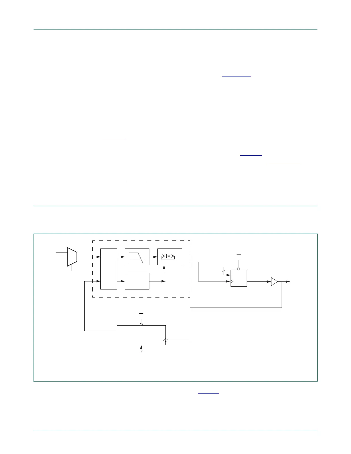
3.10 System PLL/USB PLL functional description
The LPC11U3x/2x/1x uses the system PLL to create the clocks for the core and
peripherals. An identical PLL is available for the USB.
The block diagram of this PLL is shown in Figure 9. The input frequency range is 10 MHz
to 25 MHz. The input clock is fed directly to the Phase-Frequency Detector (PFD). This
block compares the phase and frequency of its inputs, and generates a control signal
when phase and/ or frequency do not match. The loop filter filters these control signals
and drives the current controlled oscillator (CCO), which generates the main clock and
(1) System PLL only.
Fig 9. System PLL block diagram
LOCK
DETECT
PFD
FCLKOUT
pd
analog section
pd
cd
/M
/2P
cd
PSEL<1:0>
pd
2
MSEL<4:0>
5
irc_osc_clk
(1)
sys_osc_clk
SYSPLLCLKSEL/
USBPLLCLKCEL
FCLKIN
FCCO
LOCK

 Loading...


