UM10462 All information provided in this document is subject to legal disclaimers. © NXP B.V. 2016. All rights reserved.
User manual Rev. 5.5 — 21 December 2016 288 of 523
NXP Semiconductors
UM10462
Chapter 13: LPC11U3x/2x/1x SSP/SPI
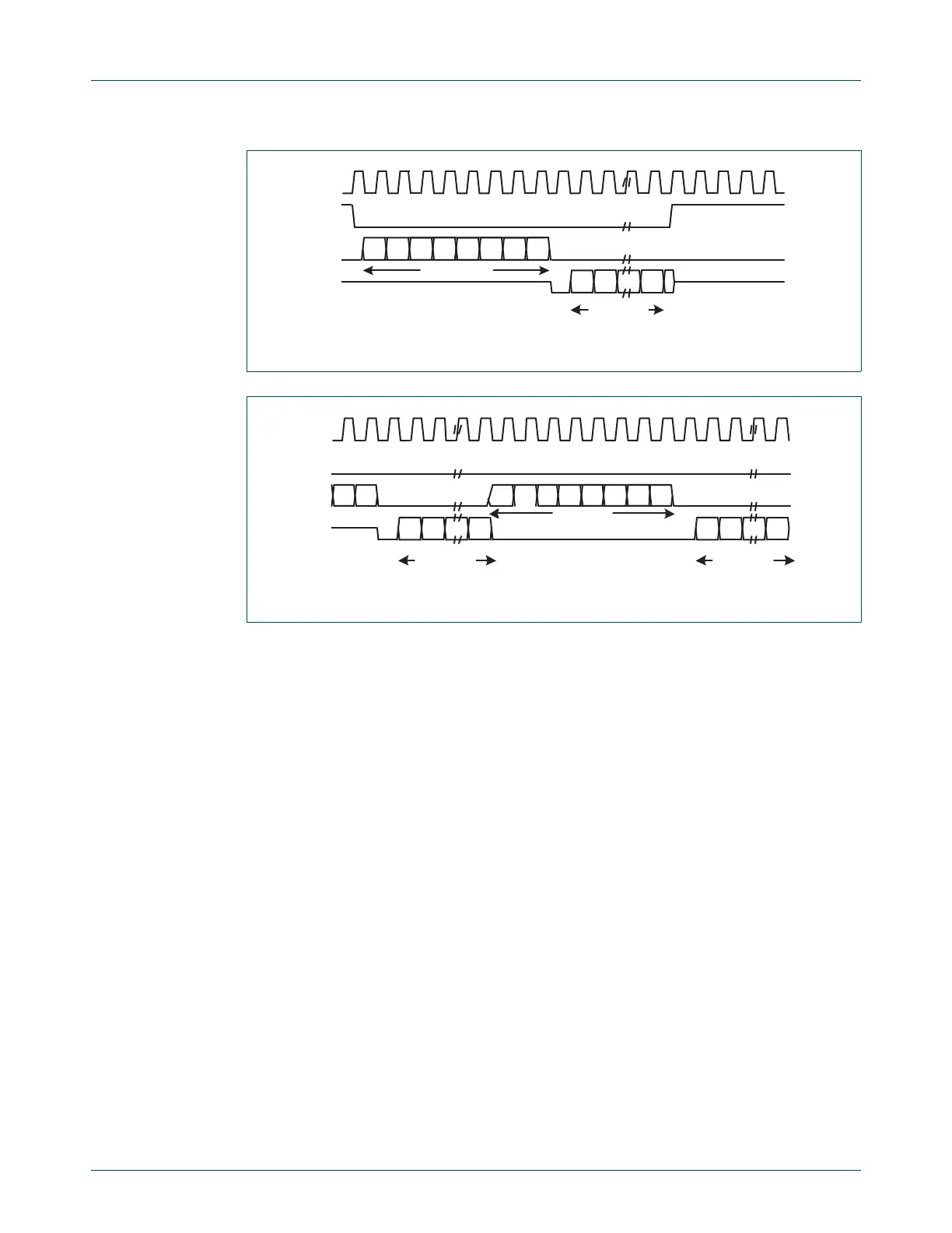
Microwire format is very similar to SPI format, except that transmission is half-duplex
instead of full-duplex, using a master-slave message passing technique. Each serial
transmission begins with an 8-bit control word that is transmitted from the SSP/SPI to the
off-chip slave device. During this transmission, no incoming data is received by the
SSP/SPI. After the message has been sent, the off-chip slave decodes it and, after
waiting one serial clock after the last bit of the 8-bit control message has been sent,
responds with the required data. The returned data is 4 to 16 bit in length, making the total
frame length anywhere from 13 to 25 bits.
In this configuration, during idle periods:
• The SK signal is forced LOW.
• CS is forced HIGH.
• The transmit data line SO is arbitrarily forced LOW.
A transmission is triggered by writing a control byte to the transmit FIFO.The falling edge
of CS causes the value contained in the bottom entry of the transmit FIFO to be
transferred to the serial shift register of the transmit logic, and the MSB of the 8-bit control
frame to be shifted out onto the SO pin. CS remains LOW for the duration of the frame
transmission. The SI pin remains tri-stated during this transmission.
The off-chip serial slave device latches each control bit into its serial shifter on the rising
edge of each SK. After the last bit is latched by the slave device, the control byte is
decoded during a one clock wait-state, and the slave responds by transmitting data back
to the SSP/SPI. Each bit is driven onto SI line on the falling edge of SK. The SSP/SPI in
Fig 37. Microwire frame format (single transfer)
Fig 38. Microwire frame format (continuous transfers)
SK
CS
SO
4 to 16 bits
of output data
SI
8-bit control
MSB LSB
0
MSB LSB
SK
CS
SO
SI
MSB LSB
4 to 16 bits
of output data
8-bit control
4 to 16 bits
of output data
MSB LSB
0
MSB LSB
LSB

 Loading...


