UM10462 All information provided in this document is subject to legal disclaimers. © NXP B.V. 2016. All rights reserved.
User manual Rev. 5.5 — 21 December 2016 426 of 523
NXP Semiconductors
UM10462
Chapter 21: LPC11U3x/2x/1x Serial Wire Debugger (SWD)
21.6.3 Boundary scan
The RESET pin selects between the JTAG boundary scan (RESET = LOW) and the ARM
SWD debug (RESET
= HIGH). The ARM SWD debug port is disabled while the
LPC11U3x/2x/1x is in reset.
To perform boundary scan testing, follow these steps:
1. Erase any user code residing in flash.
2. Power up the part with the RESET
pin pulled HIGH externally.
3. Wait for at least 250 s.
4. Pull the RESET
pin LOW externally.
5. Perform boundary scan operations.
6. Once the boundary scan operations are completed, assert the TRST pin to enable the
SWD debug mode and release the RESET
pin (pull HIGH).
Remark: The JTAG interface cannot be used for debug purposes.
Remark: POR, BOD reset, or a LOW on the TRST pin puts the test TAP controller in the
Test-Logic Reset state. The first TCK clock while RESET
= HIGH places the test TAP in
Run-Test Idle mode.
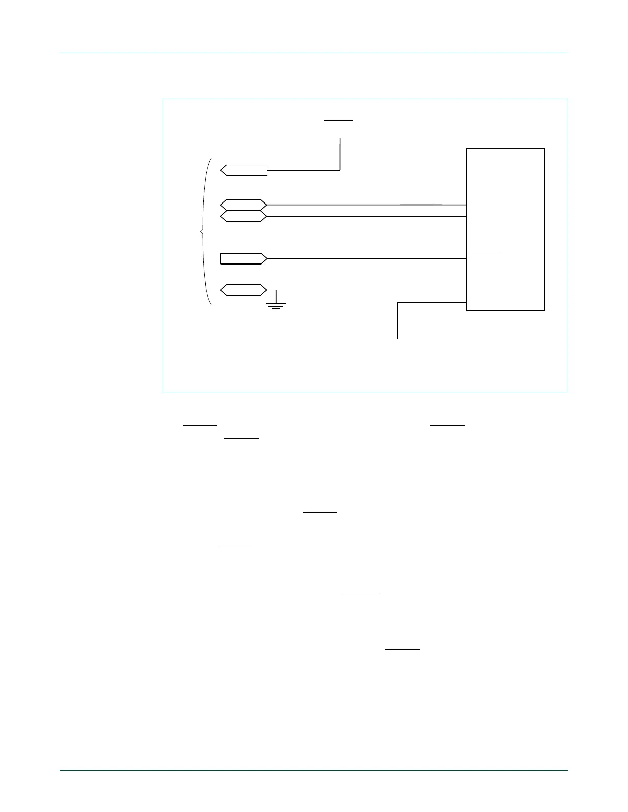
The VTREF pin on the SWD connector enables the debug connector to match the target voltage.
Fig 72. Connecting the SWD pins to a standard SWD connector
RESET
Signals from SWD connector
SWDIO
SWCLK
VDD
Gnd
VTREF
SWDIO
SWCLK
nSRST
GND
LPC11Uxx
ISP entry
PIO0_1

 Loading...


