7–14 Altera Corporation
Stratix Device Handbook, Volume 2 September 2004
Finite Impulse Response (FIR) Filters
Figure 7–7. Block Diagram of 8-Tap FIR Filter with TDM Factor of n=2
TDM Filter Implementation
TDM FIR filters are implemented in Stratix and Stratix GX devices by
configuring the DSP blocks in the multiplier-adder mode. Figure 7–9
shows the implementation of an 8-tap TDM FIR filter (n=2) with 18 bits
of data and coefficient inputs. Because the input data needs to be loaded
into the DSP block in parallel, a shift register chain is implemented using
a combination of logic cells and the altshift_taps function. This shift
register is clocked with the same data sample rate (clock 1
× ). The filter
coefficients are stored in ROM and loaded into the DSP block in parallel
as well. Because the TDM factor is 2, both the ROM and DSP block are
clocked with clock 2
× .
Figure 7–8 and Table 7–7 show the coefficient loading schedule. For
example, during cycle 0, only the flip-flops corresponding to h(1), h(3),
h(5), and h(7) are enabled. This produces the temporary output, y
0
, which
is stored in a flip-flop outside the DSP block. During cycle 1, only the flip-
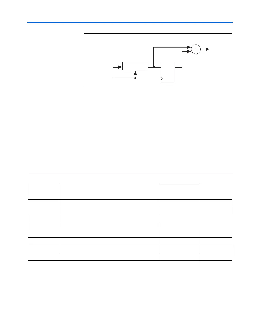
D Q
FIR filter with
four multipliers
18-bit input
2x clock
Output
Table 7–7. Operation of TDM Filter (Shown in Figure 7–9 on page 7–16)
Cycle of
2
× Clock
Cycle Output Operation
Overall Output,
y(n)
0 y
0
= x(n-1)h(1) + x(n-3)h(3) + x(n-5)h(5) + x(n-7)h(7) Store result N/A
1 y
1
= x(n)h(0) + x(n-2)h(2) + x(n-4)h(4) + x(n-6)h(6) Generate output y(n) = y
0
+ y
1
2 y
2
= x(n)h(1) + x(n-2)h(3) + x(n-4)h(5) + x(n-6)h(7) Store result N/A
3 y
3
= x(n+1)h(0) + x(n-1)h(2) + x(n-3)h(4) + x(n-5)h(6) Generate output y(n) = y
2
+ y
3
4 y
4
= x(n+1)h(1) + x(n-1)h(3) + x(n-3)h(5) + x(n-5)h(7) Store result N/A
5 y
5
= x(n+2)h(0) + x(n)h(2) + x(n-2)h(4) + x(n-4)h(6) Generate output y(n) = y
4
+ y
5
6 y
6
= x(n+2)h(1) + x(n)h(3) + x(n-2)h(5) + x(n-4)h(7) Store result N/A
7 y
7
= x(n+3)h(0) + x(n+1)h(2) + x(n-1)h(4) + x(n-3)h(6) Generate output y(n) = y
6
+ y
7