7–30 Altera Corporation
Stratix Device Handbook, Volume 2 September 2004
Finite Impulse Response (FIR) Filters
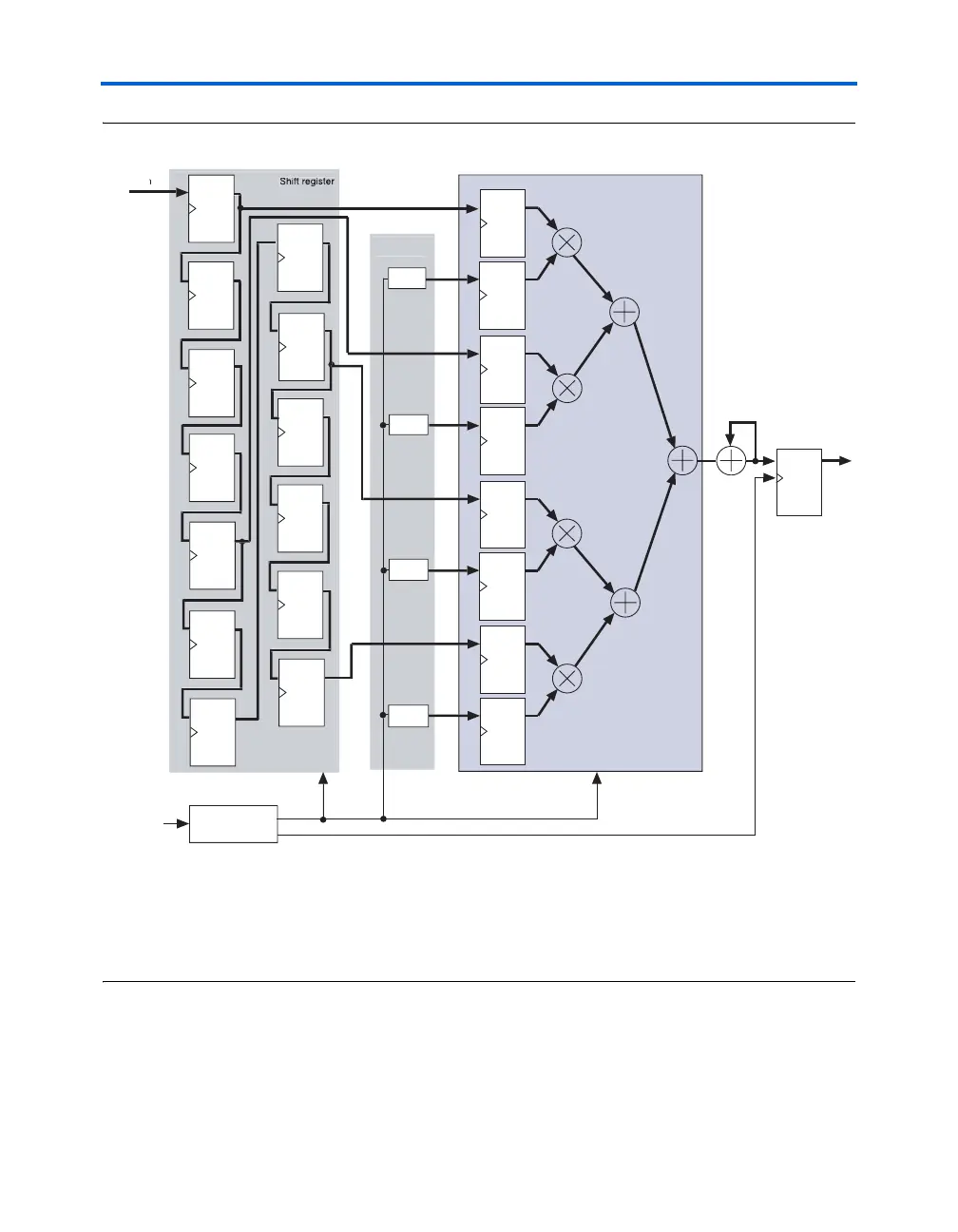
Figure 7–17. Implementation of the Polyphase Decimation Filter (D=4) Notes (1), (2), (3)
Notes to Figure 7–17:
(1) The 1× clock feeds the register after the accumulator block.
(2) The 4× clock feeds the shift register for the data, the input registers for both the data and filter coefficients, the other
optional registers in the DSP block (see Note (3)), and the accumulator block.
(3) To increase the DSP block performance, include the pipeline, and output registers. See Figure 7–3 on page 7–8 for
the details.
Filter output
y(n)
Note (2)
Clock input
(1x clock)
R
R
R
M
R
1x clock
PLL
DQ
DQ
DQ
DQ
DQ
DQ
DQ
DQ
4x clock
Note (1)
DSP block
Filt
r
o
ffi
i
nt
ata
n
u
D
Q