Altera Corporation 8–11
July 2005 Stratix Device Handbook, Volume 2
Implementing 10-Gigabit Ethernet Using Stratix & Stratix GX Devices
AC Timing Specifications
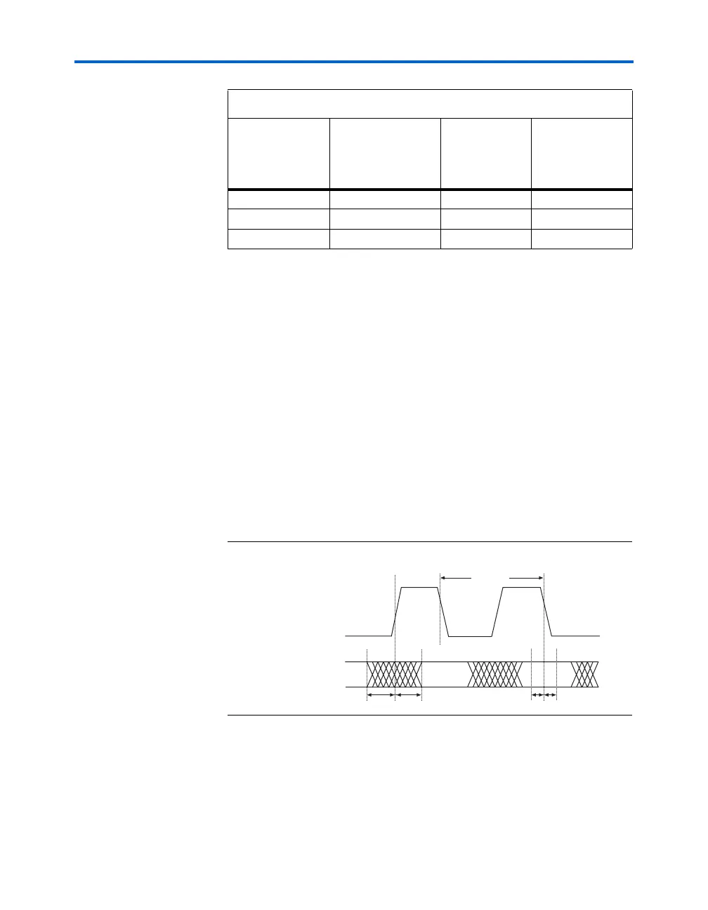
Stratix and Stratix GX devices support a PCS interface. Figures 8–8 and
8–9 and Tables 8–4 and 8–5 illustrate timing characteristics of the PCS
transmitter and receiver interfaces.
Figure 8–8 shows the AC timing diagram for the Stratix and Stratix GX
PCS transmitter. You can determine PCS channel-to-channel skew by
adding the data invalid window before the rising edge (T
cq_pre
) to the data
invalid window after the rising edge (T
cq_post
).
Figure 8–8. PCS Transmitter Timing Diagram
Table 8–3. Stratix GX Device XSBI Core Support
Stratix GX Device
Number of LVDS
Channels
(Receive/Transmit)
(1)
Number of Fast
PLLs
Number of XSBI
Interfaces
(Maximum)
EP1SGX10 22/22 2 1
EP1SGX25 39/39 2 2
EP1SGX40 45/45 4 2
Note to Ta b le 8 – 3 :
(1) The LVDS channels can go up to 840 Mbps for flip-chip packages and up to
624 Mbps for wire-bond packages. This number includes both high speed and
low speed channels. The high speed LVDS channels can go up to 840 Mbps. The
low speed LVDS channels can go up to 462 Mbps. The High-Speed Differential I/O
Support chapter in the Stratix Device Handbook, Volume 1, and the device pin-outs
on the web (www.altera.com) specify which channels are high and low speed.
T
period
T
cq_pre
T
cq_post
T
setup
T
hold
Valid
Data
TX_DATA[15..0]
PMA_TX_CLK