Altera Corporation 11–15
July 2005 Stratix Device Handbook, Volume 2
Configuring Stratix & Stratix GX Devices
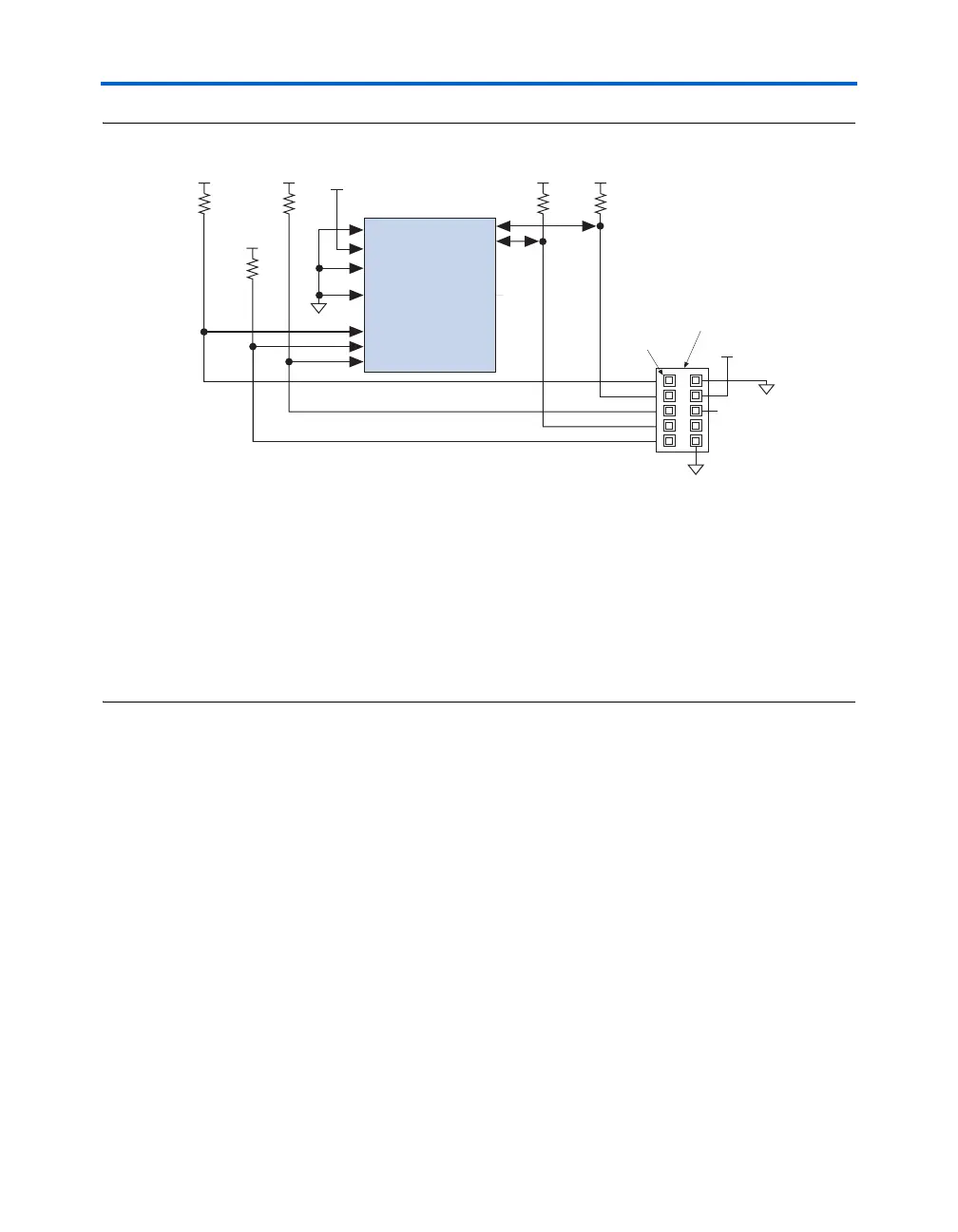
Figure 11–5. PS Configuration Circuit with a Download Cable
Notes to Figure 11–5:
(1) You should connect the pull-up resistor to the same supply voltage as the MasterBlaster (VIO pin) or ByteBlasterMV
cable.
(2) The pull-up resistors on the DATA0 and DCLK pins are only needed if the download cable is the only configuration
scheme used on the board. This is to ensure that the DATA0 and DCLK pins are not left floating after configuration.
For example, if the design also uses a configuration device, the pull-up resistors on the DATA0 and DCLK pins are
not necessary.
(3) Pin 6 of the header is a V
IO
reference voltage for the MasterBlaster output driver. V
IO
should match the device’s
V
CCIO
. This pin is a no-connect pin for the ByteBlasterMV header.
You can use programming hardware to configure multiple Stratix and
Stratix GX devices by connecting each device’s nCEO pin to the
subsequent device’s nCE pin. All other configuration pins are connected
to each device in the chain.
Because all CONF_DONE pins are tied together, all devices in the chain
initialize and enter user mode at the same time. In addition, because the
nSTATUS pins are tied together, the entire chain halts configuration if any
device detects an error. In this situation, the Quartus II software must
restart configuration; the Auto-Restart Configuration on Frame Error
option does not affect the configuration cycle.
Figure 11–6 shows how to configure multiple Stratix and Stratix GX
devices with a MasterBlaster or ByteBlasterMV cable.
Download Cable
10-Pin Male Header
(PS Mode)
V
CC
(1)
V
CC
(1)
V
CC
V
CC
(1)
V
CC
(1)
V
CC
(1)
Stratix or
Stratix GX Device
MSEL2
DCLK
nCONFIG
CONF_DONE
Shield
GND
MSEL1
MSEL0
10 kΩ10 kΩ10 kΩ
10 kΩ
10 kΩ
nSTATUS
DATA0
Pin 1
nCE
GND
GND
VIO
(3)
V
CC
(2)(2)
(2)
nCEO N.C.