UM10462 All information provided in this document is subject to legal disclaimers. © NXP B.V. 2016. All rights reserved.
User manual Rev. 5.5 — 21 December 2016 131 of 523
NXP Semiconductors
UM10462
Chapter 8: LPC11U3x/2x/1x Pin configuration
Fig 17. Pin configuration (TFBGA48)
002aag101_1
LPC11U1x/3x
Transparent top view
H
G
F
D
B
E
C
A
24681357
ball A1
index area
See Table 134 for the full pin name.
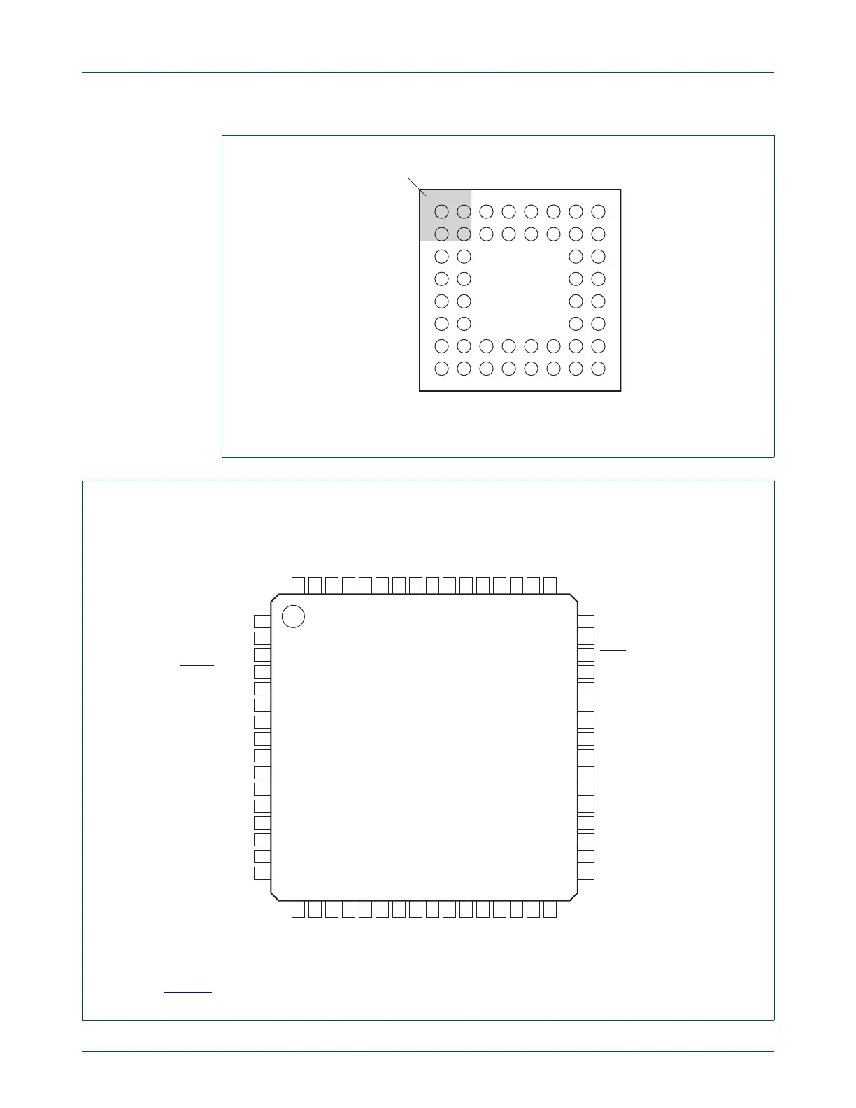
Fig 18. Pin configuration (LQFP64)
LPC11U2x
LPC11U3x
PIO1_0 V
DD
PIO1_25 PIO1_13
PIO1_19 TRST/PIO0_14
RESET/PIO0_0 TDO/PIO0_13
PIO0_1 TMS/PIO0_12
PIO1_7 PIO1_11
V
SS
TDI/PIO0_11
XTALIN PIO1_29
XTALOUT PIO0_22
V
DD
PIO1_8
PIO0_20 SWCLK/PIO0_10
PIO1_10 PIO0_9
PIO0_2 PIO0_8
PIO1_26 PIO1_21
PIO1_27 PIO1_2
PIO1_4 V
DD
PIO1_1 PIO1_6
PIO1_20 PIO1_16
PIO0_3 PIO0_19
PIO0_4 PIO0_18
PIO0_5 PIO0_17
PIO0_21 PIO1_12
PIO1_17 V
DD
PIO1_23 PIO1_15
USB_DM PIO0_23
USB_DP PIO1_9
PIO1_24 V
SS
PIO1_18 PIO0_16
PIO0_6 SWDIO/PIO0_15
PIO0_7 PIO1_22
PIO1_28 PIO1_3
PIO1_5 PIO1_14
002aag624_1
1
2
3
4
5
6
7
8
9
10
11
12
13
14
15
16
48
47
46
45
44
43
42
41
40
39
38
37
36
35
34
33
17
18
19
20
21
22
23
24
25
26
27
28
29
30
31
32
64
63
62
61
60
59
58
57
56
55
54
53
52
51
50
49

 Loading...


