UM10462 All information provided in this document is subject to legal disclaimers. © NXP B.V. 2016. All rights reserved.
User manual Rev. 5.5 — 21 December 2016 435 of 523
NXP Semiconductors
UM10462
Chapter 24: LPC11U3x/2x/1x Appendix ARM Cortex-M0
[1] Describes access type during program execution in thread mode and Handler mode. Debug access can
differ.
[2] Bit[24] is the T-bit and is loaded from bit[0] of the reset vector.
24.3.1.3.1 General-purpose registers
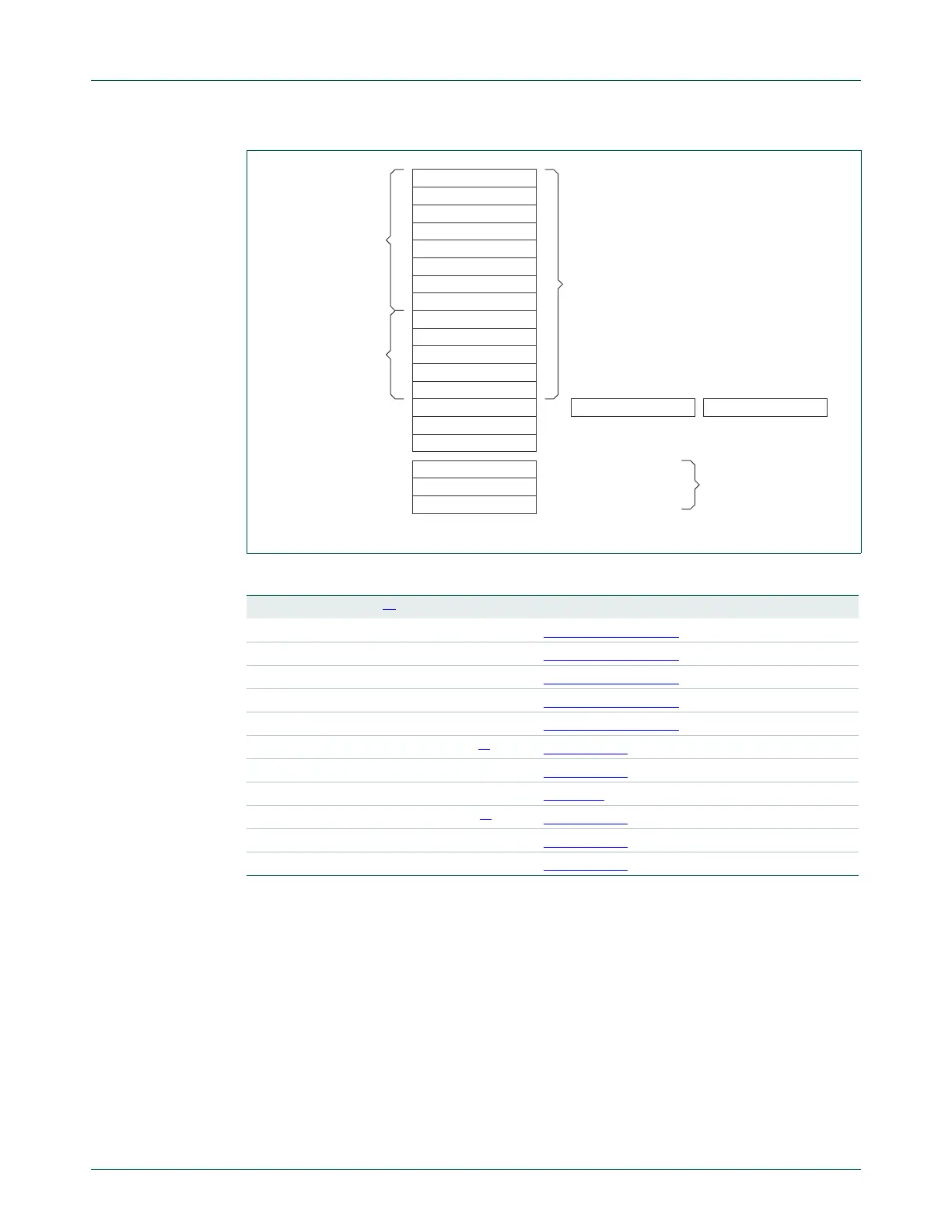
R0-R12 are 32-bit general-purpose registers for data operations.
24.3.1.3.2 Stack Pointer
The Stack Pointer (SP) is register R13. In Thread mode, bit[1] of the CONTROL register
indicates the stack pointer to use:
• 0 = Main Stack Pointer (MSP). This is the reset value.
• 1 = Process Stack Pointer (PSP).
Fig 75. Processor core register set
Table 413. Core register set summary
Name Type
[1]
Reset value Description
R0-R12 RW Unknown Section 24–24.3.1.3.1
MSP RW See description Section 24–24.3.1.3.2
PSP RW Unknown Section 24–24.3.1.3.2
LR RW Unknown Section 24–24.3.1.3.3
PC RW See description Section 24–24.3.1.3.4
PSR RW Unknown
[2]
Table 24–414
APSR RW Unknown Table 24–415
IPSR RO
0x00000000
Table 416
EPSR RO Unknown
[2]
Table 24–417
PRIMASK RW
0x00000000
Table 24–418
CONTROL RW
0x00000000
Table 24–419
3URJUDP&RXQWHU
635
/55
3&5
5
5
5
5
5
5
5
5
5
5
5
5
5
/RZUHJLVWHUV
+LJKUHJLVWHUV
063363
&21752/
365
/LQN5HJLVWHU
6WDFN3RLQWHU
*HQHUDOSXUSRVHUHJLVWHUV
3URJUDP6WDWXV5HJLVWHU
&RQWURO5HJLVWHU
6SHFLDOUHJLVWHUV
35,0$6. ,QWHUUXSWPDVNUHJLVWHU

 Loading...


