Virtex-6 FPGA GTX Transceivers User Guide www.xilinx.com 307
UG366 (v2.5) January 17, 2011
17h
15
R/W
GEN_RXUSRCLK
FALSE
0
TRUE 1
14:12 RX_DATA_WIDTH 2:0
20
011
8 000
10 001
16 010
32 100
40 101
11 CHAN_BOND_SEQ_2_CFG 4 <4:0> 0-31 1
(1)
10 BIAS_CFG 16
9:5 RX_CLK25_DIVIDER 4:0
6
00101
1 00000
2 00001
3 00010
4 00011
5 00100
7 00110
8 00111
9 01000
10 01001
11 01010
12 01011
13 01100
14 01101
15 01110
16 01111
17 10000
18 10001
19 10010
20 10011
21 10100
22 10101
23 10110
24 10111
25 11000
26 11001
27 11010
28 11011
29 11100
30 11101
31 11110
32 11111
4 AC_CAP_DIS
FALSE
0
TRUE 1
3 GTX_CFG_PWRUP
FALSE
0
TRUE 1
2:0 OOBDETECT_THRESHOLD 2:0 0-7 1
(1)
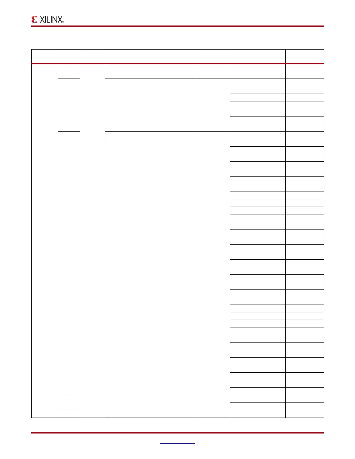
Table B-1: Attributes DRP Address Map (Cont’d)
DADDR
DRP Bits R/W Attribute Name Attribute Bits Attribute Encoding
DRP Binary
Encoding

 Loading...
