20 www.xilinx.com Virtex-6 FPGA GTX Transceivers User Guide
UG366 (v2.5) January 17, 2011
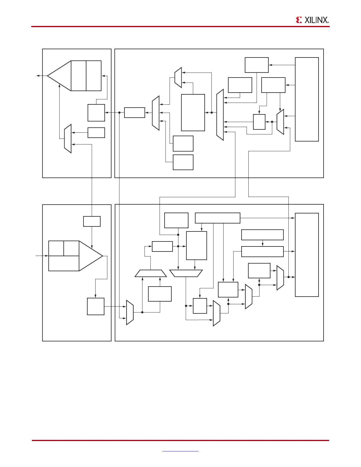
Chapter 1: Transceiver and Tool Overview
Details about the different functional blocks of the transmitter and receiver including their
use models are described in Chapter 3, Transmitter, and Chapter 4, Receiver.
Figure 1-2 shows the GTX transceiver placement in an example Virtex-6 device
(XC6VLX75T).
Additional information on the functional blocks in Figure 1-2 is available in the following
locations:
X-Ref Target - Figure 1-1
Figure 1-1: Virtex-6 FPGA GTX Transceiver Simplified Block Diagram
TX-PMA TX-PCS
FPGA
TX
Interface
TX
Gearbox
UG366_c1_01_051509
TX PIPE
Control
Phase
Adjust
FIFO &
Over-
sampling
PCIe
Beacon
From RX Parallel Data
(Far-End PMA Loopback)
To RX Parallel
Data (Near-End
PCS Loopback)
From RX Parallel Data
(Far-End PCS Loopback)
PISO
TX
Pre/
Post
emp
PLL
TX
OOB
and
PCIe
TX
Driver
Polarity
Polarity
SATA
OOB
8B/
10B
Pattern
Generator
RX-PMA RX-PCS
FPGA
RX
Interface
Loss of Sync
RX PIPE Control
RX Status Control
SIPO
PLL
RX
EQ
DFE
RX OOB
RX
CDR
RX
Gearbox
Over-
sampling
Elastic
Buffer
Pattern
Checker
Comma
Detect
and
Align
10B
/8B

 Loading...

