252 www.xilinx.com Virtex-6 FPGA GTX Transceivers User Guide
UG366 (v2.5) January 17, 2011
Chapter 4: Receiver
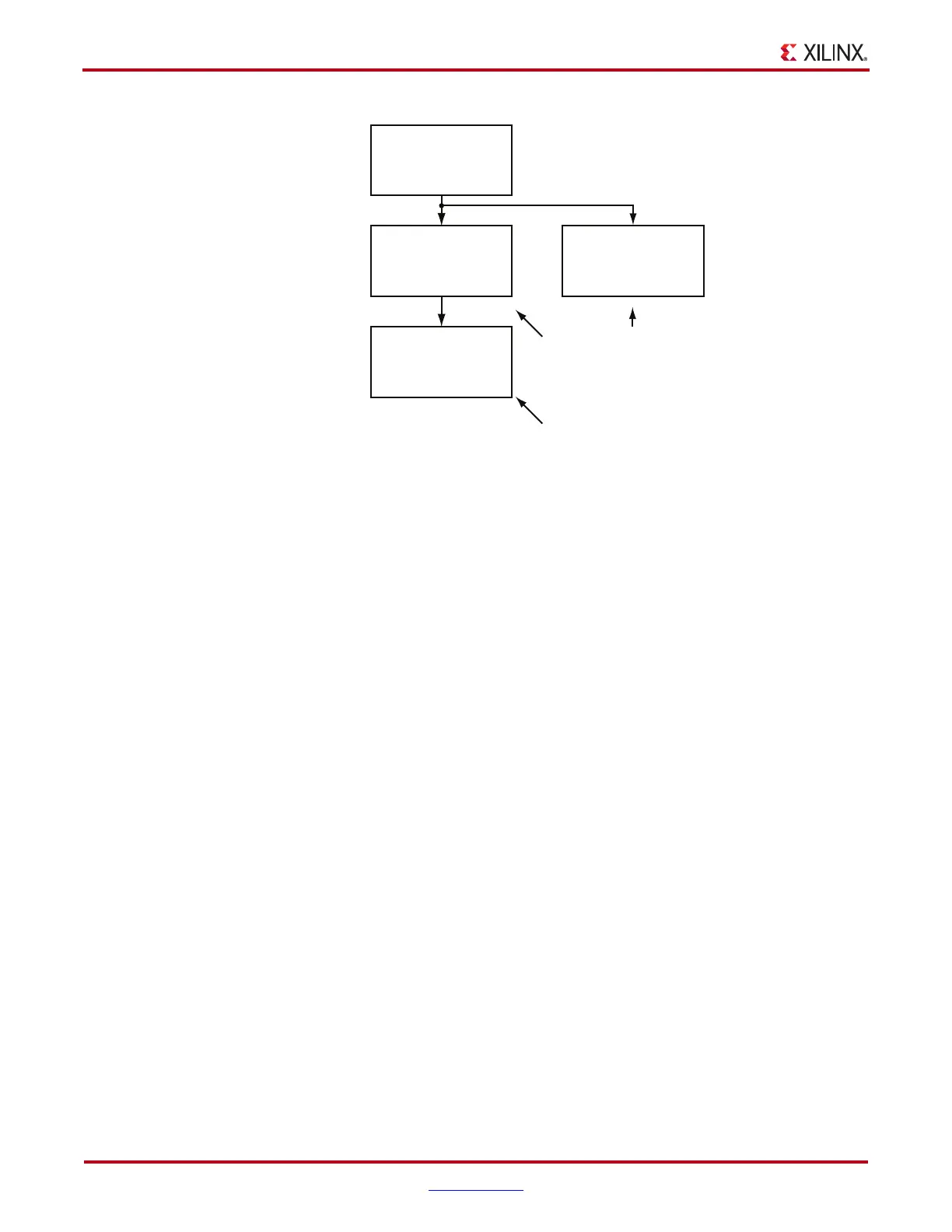
To set up a daisy chain, first connect the GTX transceivers using RXCHBONDO and
RXCHBONDI to create a path from the RXCHBONDI port of each slave to the
RXCHBONDO port of the master. Use the following steps to set the
RXCHANBONDLEVEL[2:0] for the GTX transceivers in the chain:
1. Set the RXCHANBONDLEVEL[2:0] of the master to 7.
2. Set the RXCHANBONDLEVEL[2:0] of each slave to the RXCHANBONDLEVEL[2:0]
of the GTX transceiver driving the slave’s RXCHBONDI port minus 1.
3. Find the slave with the lowest level. Subtract this level from the
RXCHANBONDLEVEL[2:0] of all GTX transceivers so that the lowest slave has level 0
and the master has the minimum level required to service all the slaves.
Any number of GTX transceivers can be channel bonded together as long as the timing
constraints of the design are met and all clocking guidelines are followed (see Figure 2-5,
page 109).
When the connections between channel bonding ports among GTX transceivers are being
decided, the designer must remember that RXCHBONDI and RXCHBONDO belong to the
RXUSRCLK clock domain. Meeting the timing constraint of RXUSRCLK becomes
increasingly difficult as RXUSRCLK increases in frequency and as directly connected
transceivers get further apart.
Selecting a GTX transceiver in the middle of the GTX column to be the master for channel
bonding allows for the most flexibility when connecting channel bonding ports. When the
channel bonding master is in the middle of the GTX column, connections can be made to
GTX transceivers north and south of the master. This configuration allows for daisy
chaining of up GTX transceivers from one Quad above and one Quad below the channel
bonding master. Because of the GTX dedicated clock routing structure, an additional
benefit of having the channel bonding master at the center of the GTX column is that up to
12 GTX transceivers can be channel bonded together using a single clock pin pair. If more
than 12 GTX transceivers are channel bonded together, the use of additional clock pins is
required as well as using the same oscillator (see Figure 2-5, page 109).
X-Ref Target - Figure 4-40
Figure 4-40: Channel Bonding Daisy Chain Example 2
RXCHBONDI
RXCHBONDO
RXCHBONDI
RXCHBONDO
RXCHBONDI
RXCHBONDO
RXCHBONDI
RXCHBONDO
RXCHANBONDMASTER = 1
RXCHANBONDLEVEL[2:0] = 2
RXCHANBONDSLAVE = 1
RXCHANBONDLEVEL[2:0] = 1
RXCHANBONDSLAVE = 1
RXCHANBONDLEVEL[2:0] = 0
UG366_c4_37_051509

 Loading...

