3-74 Return to Section Topics 4200-900-01 Rev. K / February 2017
Section 3: Common Device Characterization Tests Model 4200-SCS User’s Manual
Configuring device stress properties
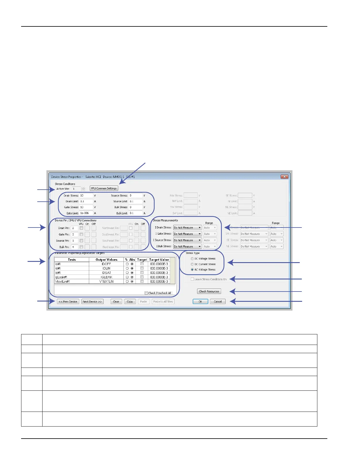
Properties for device stressing are set from the Device Stress Properties windows
(see Figure 3-59). This window is opened by clicking the Device Stress
Properties button on the Subsite Setup tab. The button is shown in Figure 3-51.
The device stress properties window that opens will be for the first device in the
subsite plan. There is a separate properties window for each device in the plan.
The properties window for each device is displayed by clicking the Next Device or
Prev Device button at the bottom of the window. The basic steps to configure
each device are provided in Figure 3-59. Details about configuration follow the
illustration.
Figure 3-59
Device Stress Properties: Setup steps for first device in Subsite Plan
Table 3-25
Setup steps for the first device in the Subsite Plan
Step Description
1 Select the wafer site number. See Multi-site testing.
2 Select DC Voltage Stress, DC Current Stress, or AC Voltage Stress. See DC voltage, DC current, or AC voltage
stressing.
3 Enter the stress values (V or I) and limit values (I or V).
4 If AC Voltage Stress was selected, select VPU Common Settings to open the window to make common settings for
the Keithley pulse card. See Setting AC stress properties.
5 Assign connection pin numbers for this device. With “AC Voltage Stress” selected, click “VPU” checkbox if connected
to the 4205-PG2.
On and Off determine the SMU sequence when powering DUTs. See Device pin connections.
6 The Degradation Targets table lists the tests and Output Values for this device. Targets can be enabled and the
Target Values can be set in % or Absolute Value. Click to enable or disable all Targets. See Degradation targets.
1
2
3
4
5
6
7
8
11
12
13
 Loading...