4200-900-01 Rev. K / February 2017 Return to Section Topics 3-89
Model 4200-SCS User’s Manual Section 3: Common Device Characterization Tests
Configure Device Stress Properties
To configure the device stress properties for the Segment / Stress Measure Mode
(see Figure 3-71):
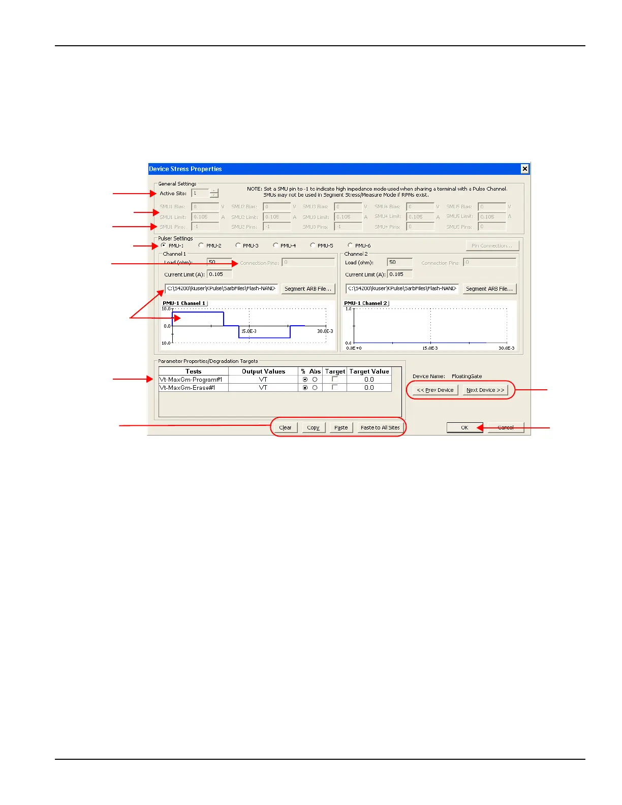
Figure 3-71
Segment Stress / Measure Mode: Device Stress Properties
1.Active Site selection:
• When active, this field is used to select the wafer site number.
• If there is only one wafer site, this field will be inactive.
2.Pulser selection:
• There is a Device Settings Properties window for each pulse generator card in the system
(Model 4225-PMU, 4220-PGU, 4205-PG2, or 4200-PG2).
• Select the pulser to be configured.
3.SMU Pins:
• No switch matrix:
– With no switch matrix, the active SMU pin fields must be set to 0 (no connection) or -
1 (high impedance).
– The -1 setting puts the SMU in a high impedance mode, which is necessary if it
shares a pin with a VPU.
• Switch matrix:
– With a switch matrix added to the system, the pin number settings determine signal
routing for the SMUs through the matrix to the device pins.
4.PG2 Matrix connections:
• With a switch matrix added to the system, fields for PG2 Channel pins are active.
– There is a PG2 pin connection setting each channel.
• The pin number settings determine signal routing for the PG2 Channels through the
matrix to the device pins.
 Loading...