3-78 Return to Section Topics 4200-900-01 Rev. K / February 2017
Section 3: Common Device Characterization Tests Model 4200-SCS User’s Manual
How to perform AC stress for wafer level reliability (WLR)
AC, or pulsed, stress is a useful addition to the typical stress-measure tests for
investigating both semiconductor charge trapping and degradation behaviors.
NBTI (negative bias temperature instability) and TDDB (time dependent dielectric
breakdown) tests consist of stress / measure cycles.
The applied stress voltage is a DC signal, which is used because it maps more
easily to device models. However, incorporating pulsed stress testing provides
additional data that permits a better understanding of device performance in
frequency-dependent circuits.
NOTE Key test parameters are contained in Table 3-26.
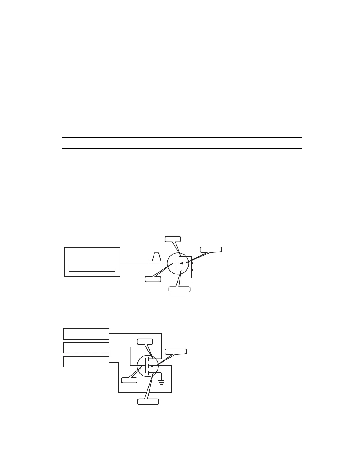
1. Connect pulse generator to DUT during stress as shown in Figure 3-62, Figure 3-63, and
Figure 3-64.
2. The test pulse stresses the device for HCI, NBTI and TDDB test instead of DC bias by
outputting a train of pulses for a period of time (stress time). Pulse characteristics are not
changed during the stress-measure test.
3. The test then measures device characteristics using SMUs: Vth, Gm, and so on.
Figure 3-62
AC Pulse stress-measure—hardware setup block diagram
4200-SMU (2)
4200-SMU (1)
4200-SMU (3)
Measure
Stress
4205-PG2
Pulse Generator
V
g
Output
V
DD
Source
Drain
Substrate
Source
Drain
Substrate
Gate
Gate
 Loading...