3-156 Return to Section Topics 4200-900-01 Rev. K / February 2017
Section 3: Common Device Characterization Tests Model 4200-SCS User’s Manual
How to perform a Charge Trapping test
NOTE The chargetrapping project uses the 4205-PG2 pulse generator card and
4200-SCP2 scope card. The 4225-PMU can also be used for charge trapping (see
Reference manual, chargepumping user library, page 16-124).
Slow single pulse charge trapping high K gate stack
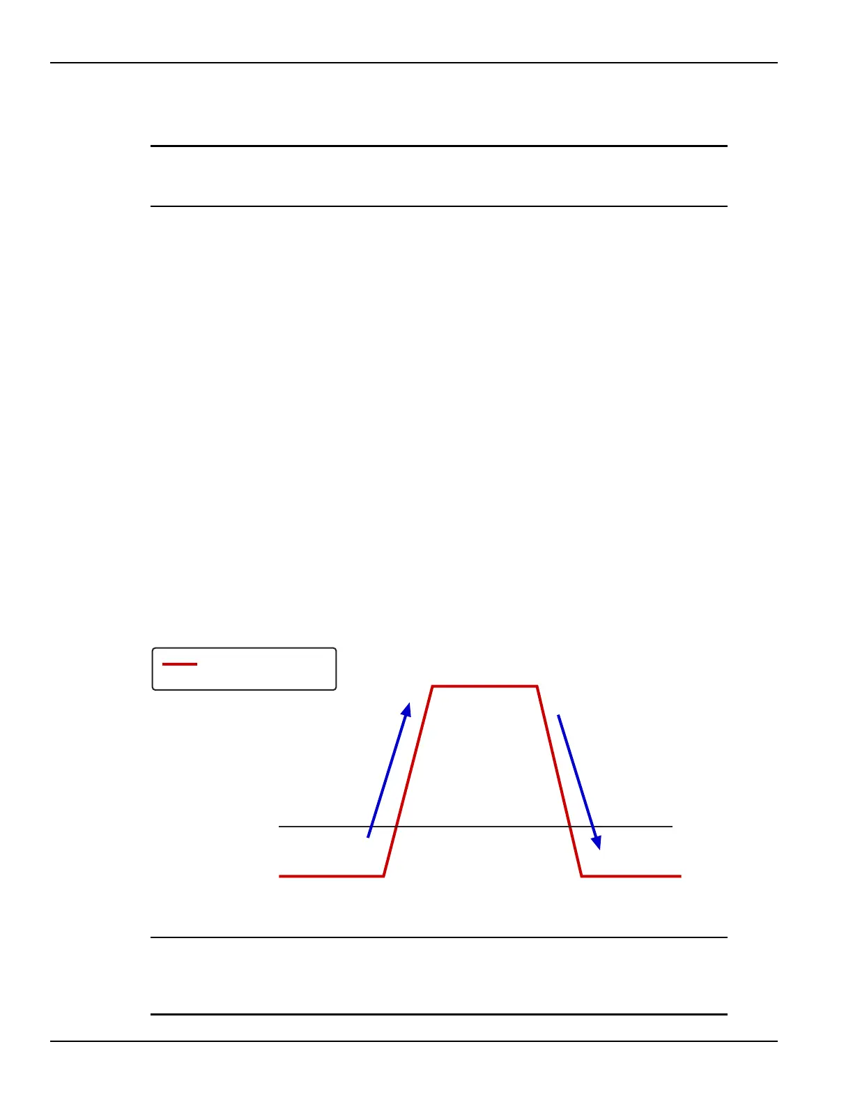
The key to using the single pulse method is to look at the charge trapping and de-
trapping behavior within a single, well-configured gate pulse (see Figure 3-124).
The gate pulse usually starts in a position that discharges the gate capacitor
before the voltage ramp begins.
This is to clean up any residual charges that might be trapped in the gate. Then,
during the rise time of the voltage ramp, the corresponding drain current response
is captured, allowing a Vgs-Id curve to be formed.
Slow single pulse refers to rise and fall transition times of 100 ns minimum, with a
pulse width of at least 1 μs.
These relatively slow pulse parameters mean that the RBT are not used and a
simple splitter can be used for monitoring the drain current pulse.
For each measurement, a pulse is applied to the gate of the transistor while its
drain is biased at a certain voltage. The change in drain current, resulting from the
gate pulse, appears on the digital oscilloscope.
Figure 3-124
Trapping and de-trapping in a single gate voltage pulse
NOTE The Charge Trapping project provides two capabilities: Slow charge trapping on a
device and the ability to perform relatively generic transient IV tests on a device. The
time-based voltages for the gate signal need to be multiplied by 1.33 if the power
divider is used as shown in Figure 3-125.
0V
Up Trace
Trapping
Down Trace
Trapping
Charge Trapping during
transistor on
De-trap before ramp
Clean up interface charges
Gate Voltage Pulse