4200-900-01 Rev. K / February 2017 Return to Section Topics 3-157
Model 4200-SCS User’s Manual Section 3: Common Device Characterization Tests
Charge trapping procedure
1. Perform cable correction (open and through, if necessary), with calibration substrate. Open
and through correction measurements are taken and inputted into correction algorithm to
calculate cable losses.
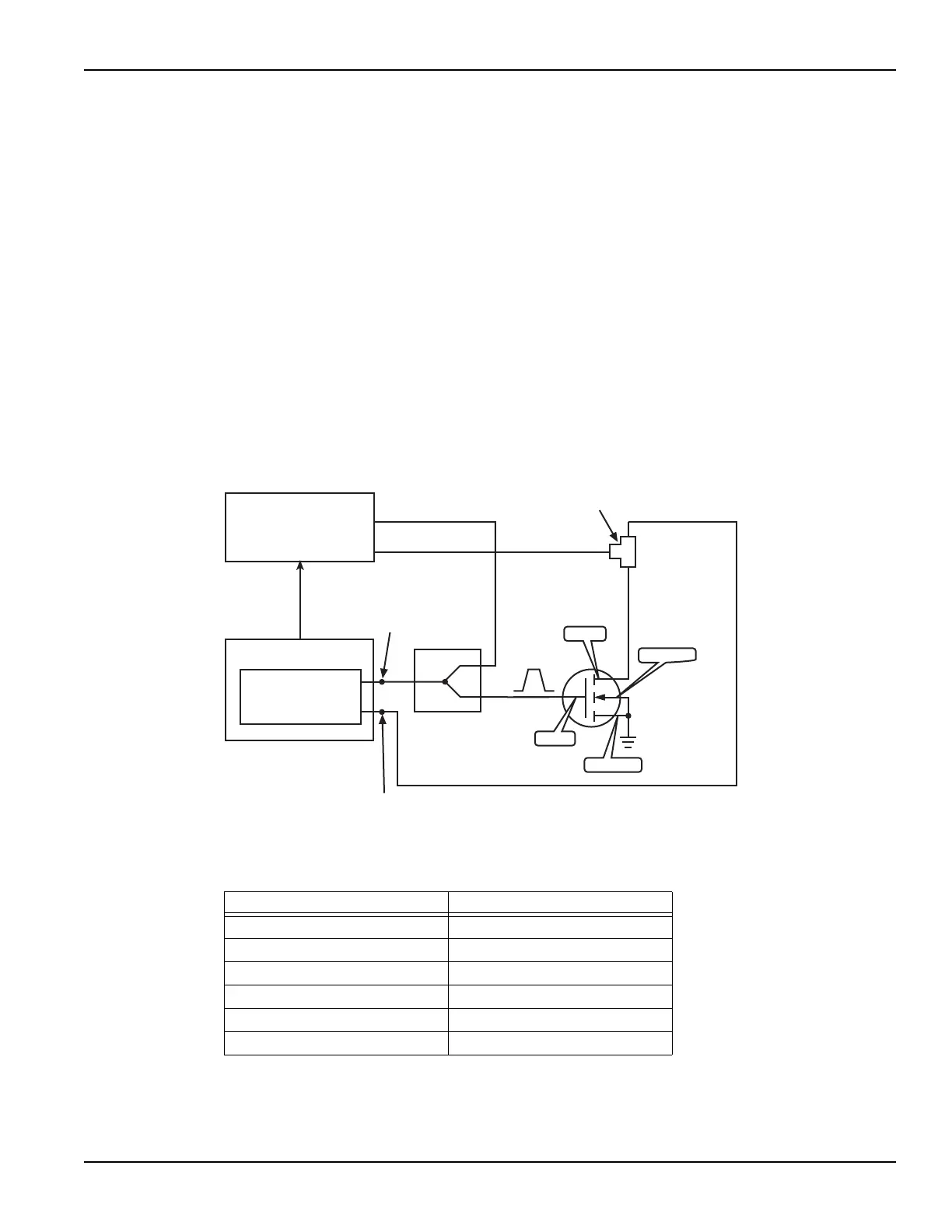
2. Connect DUT (transistor) as shown in Figure 3-125 and Figure 3-126.
3. Input test parameters, refer to key parameters contained in Table 3-32.
4. The UTM will pulse the gate with single pulse (for average >1 use a series of very low duty
cycle pulses), bias drain with a PG2, capture drain current response on oscilloscope, then
calculate corresponding drain current (Vgs-Id) from the whole waveform.
5. To ensure a determinate number of pulses are applied to the DUT, the period must be set to
>10 ms. Wider pulse widths require a longer period. If the period is too short, pulses will not
be measured and will cause the UTM to hang, requiring KITE to be manually halted.
Figure 3-125
Slow single pulse—hardware setup block diagram
Table 3-32
Key parameters—Slow Single Pulse Charge Trapping
Parameters Range/Specification
Application Pulse I-V like application
Rise / Fall time Variable 10 ns–10 μs
Pulse width 5 μs–1 ms single pulse
Pulse amplitude 0-5 V
Base voltage +/- 5 V
Load impedance 50 Ω or 1 M Ω
4200-SCP2HR
or
4200-SCP2
Scope
V
g
Channel 1
V
D
Trigger
Trigger
SMA
Splitter
Tee
4205-PG2
Pulse Generator
Channel 1
Output
Channel 2
Output
S
1
2
3-port
power
divider
Channel 2
Source
Drain
Substrate
Gate
NOTE This configuration can handle pulse widths ³ 100ns
which is too wide to use Remote Bias Tees.
 Loading...