3-82 Return to Section Topics 4200-900-01 Rev. K / February 2017
Section 3: Common Device Characterization Tests Model 4200-SCS User’s Manual
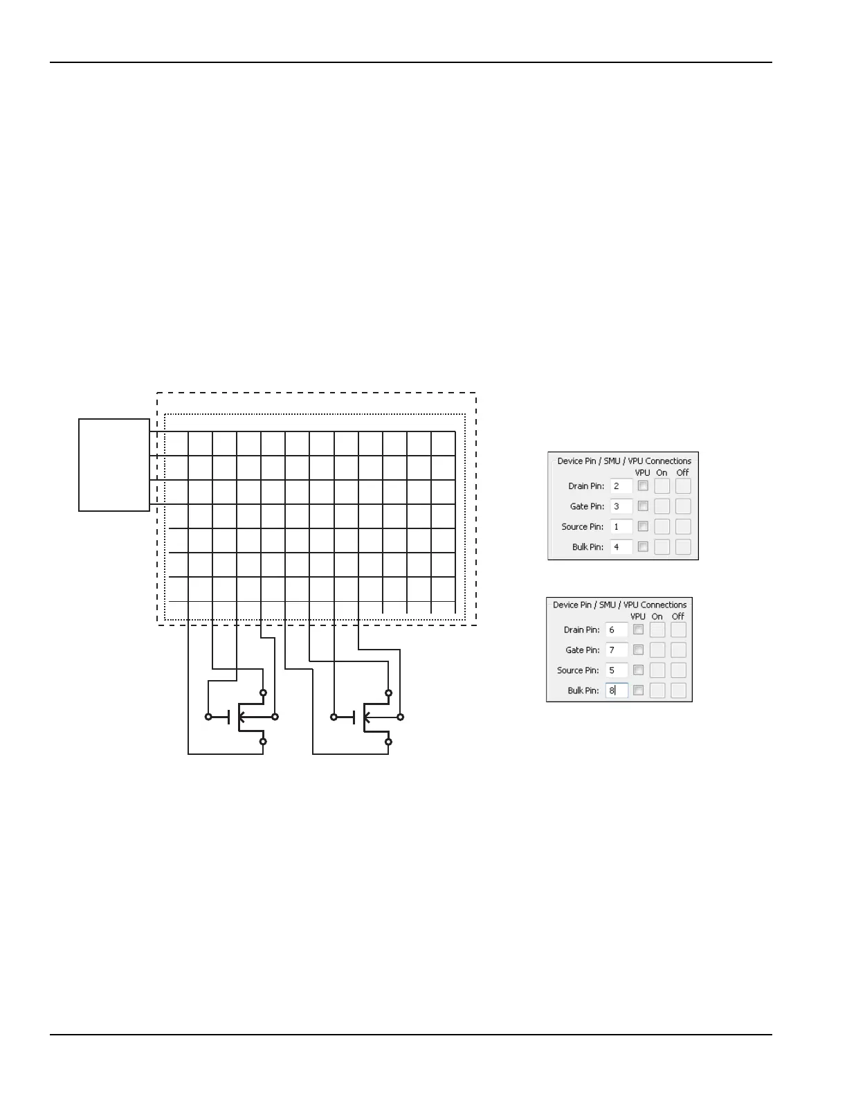
Matrix card system: For a system using a matrix card, the pin number
assignments for each device must match the actual physical connections to the
matrix card. Figure 3-65 shows an example of how the Device Pin Connections
properties must match the actual connections of the devices to the matrix card.
SMUs: If your voltage stress system is using a switch matrix, the 4200-SCS will
try to maximize the amount of SMU sharing in order to allow parallel testing. It
determines what pins can share SMUs in the following fashion. If pins from
different devices have the same name (for example, Gate Pin and Drain Pin) and
the like-named pins are assigned the same voltage stress, when the stress is
applied these pins will all be automatically connected to the same SMU through
the switch matrix. That SMU will supply the voltage stress to all the pins
simultaneously.
Figure 3-65
Example of device pin connections to a matrix card
The On and Off boxes determine the sequence the SMUs will follow for powering
DUTs. On determines the order in which the SMUs power on. If no settings are
defined, the SMUs power on from the lowest number to the highest (SMU1,
SMU2, SMU3, and so on). Off determines the sequence that SMUs will follow
when powering down DUTs (stress voltage or current goes to 0). If no settings are
defined, the SMUs power off from the lowest number to the highest (SMU1,
SMU2, SMU3, and so on).
SMU1 FORCE
SMU2 FORCE
SMU3 FORCE
SMU4 FORCE
1
2
3
4
5
6
7
8
9
10
11
12
A
B
C
D
E
F
G
H
Drain
Bulk
Source
G
Gate
Device1
Drain
Bulk
Source
G
Gate
Device2
4200-SCS
7072 Matrix Card (8 x 12)
708A Switching Mainframe
Device1 pin assignments
Device2 pin assignments
The above pin assignments must
match the actual device pin
connections to the matrix card.
Device Stress Properties
 Loading...