Signal Pin
No.
Name Function Reference
PCO
Ä
Chap.
7.10.2
‘Con-
necting an
Absolute
Linear
Encoder’
page 240
21 Encoder Divided
Pulse Output,
Phase C
Outputs the origin signal
once every encoder rota-
tion.
/PCO 22
SG 16 Signal ground This is the 0-V signal for
the control circuits.
-
FG Shell Frame ground Connected to the frame
ground if the shield of
the I/O Signal Cable is
connected to the con-
nector shell.
−
* You can change the allocations. Refer to the following section for details.
Ä
Chap. 7.2.3 ‘Output Signal Allocations’ page 198
5.6.2 I/O Signal Connector (CN1) Pin Arrangement
The following figure gives the pin arrangement of the of the I/O signal connector (CN1) for
the default settings.
The top view is from the direction of the arrow without the connector shell attached.
No Signal Specification No Signal Specification
1 /SO1+ (/BK
+)
General-purpose
Sequence Output 1
14 BAT+ Battery for Absolute
Encoder (+)
2 /SO1- (/
BK-)
General-purpose
Sequence output 1
15 BAT- Battery for Absolute
Encoder (-)
3 ALM+ Servo Alarm Output 16 SG Signal Ground
4 ALM- Servo Alarm Output 17 PAO Encoder Divided
Pulse Output,
Phase A
5 TH Overheat Protection
Input
18 /PAO Encoder Divided
Pulse Output,
Phase A
Pin 15
Pin 1
Pin 2
Pin 12
Pin 13
Pin 26
Pin 25
Pin 14
Fig. 79: Top View of I/O
Signal Connector (CN1)
Fig. 80: Side View of I/O
Signal Connector (CN1)
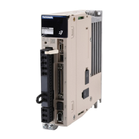
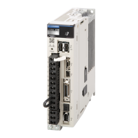
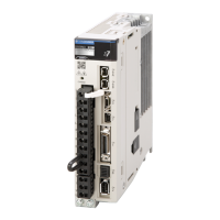
Sigma-7 Series SERVOPACKs
Wiring and Connecting SERVOPACKs
Connecting I/O Signals > I/O Signal Connector (CN1) Pin Arrangement
| | PROFINET Communications - SIEP YEUOC7P 02A Revision 0 | en | 118
 Loading...