3.3 Block Diagrams
L1
B1/ B2 B3
L2
L3
1
2
L1C
L2C
U
V
W
CN502CN11 CN12 CN7
CN2
ENC
CN5
M
CHARGE
-
+
-
-
CN8
I/O
I/F
CN1
CN6A
CN6B
Processor
(PWM control, position/
speed calculations, etc.)
Control
power
supply
Digital Operator ComputerOption Module Option Module
Current
sensor
Dynamic
brake circuit
Servomotor
Gate drive
Analog
voltage
converter
Encoder divided
pulse output
Analog monitor
output
I/O signals
Voltage
sensor
Voltage
sensor
Varistor
Varistor
Relay
drive
Gate drive
overcurrent protection
Temperature
sensor
Safety function signals
Main
circuit
power
supply
Control
power
supply
Fieldbus
communications
Status display
+
-
+
-
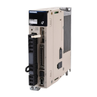
Fig. 17: Block Diagram - SGD7S-R70A, -R90A, and -1R6A
L1
B1/ B2 B3
L2
L3
1
2
L1C
L2C
U
V
W
CN502CN11 CN12 CN7
CN2
ENC
CN5
M
CHARGE
-
+
-
-
CN8
I/O
I/F
CN1
CN6A
CN6B
Processor
(PWM control, position/
speed calculations, etc.)
Control
power
supply
Digital Operator ComputerOption Module Option Module
Current
sensor
Dynamic
brake circuit
Servomotor
Gate drive
Analog
voltage
converter
Encoder divided
pulse output
Analog monitor
output
I/O signals
Voltage
sensor
Voltage
sensor
Varistor
Varistor
Relay
drive
Gate drive
overcurrent protection
Temperature
sensor
Safety function signals
Main
circuit
power
supply
Control
power
supply
Fieldbus
communications
Status display
+
-
+
-
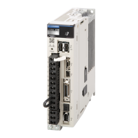
Fig. 18: Block Diagram - SGD7S-2R8A
SGD7S-R70A, -R90A, and
-1R6A
SGD7S-2R8A
Sigma-7 Series SERVOPACKs
Selecting a SERVOPACK
Block Diagrams
| | PROFINET Communications - SIEP YEUOC7P 02A Revision 0 | en | 66
 Loading...
