EasyManua.ls Logo

GigaDevice Semiconductor GD32VF103 - Table 7.8. TIMER4 Alternate Function Remapping; Table 7.9. USART0 Alternate Function Remapping; USART AF Remapping; I2 C0 AF Remapping

GigaDevice Semiconductor GD32VF103
536 pages
Print Icon
To Next Page IconTo Next Page
To Previous Page IconTo Previous Page
Loading...
GD32VF103 User Manual
110
1. For different packages and flash sizes please refer to the datasheet.
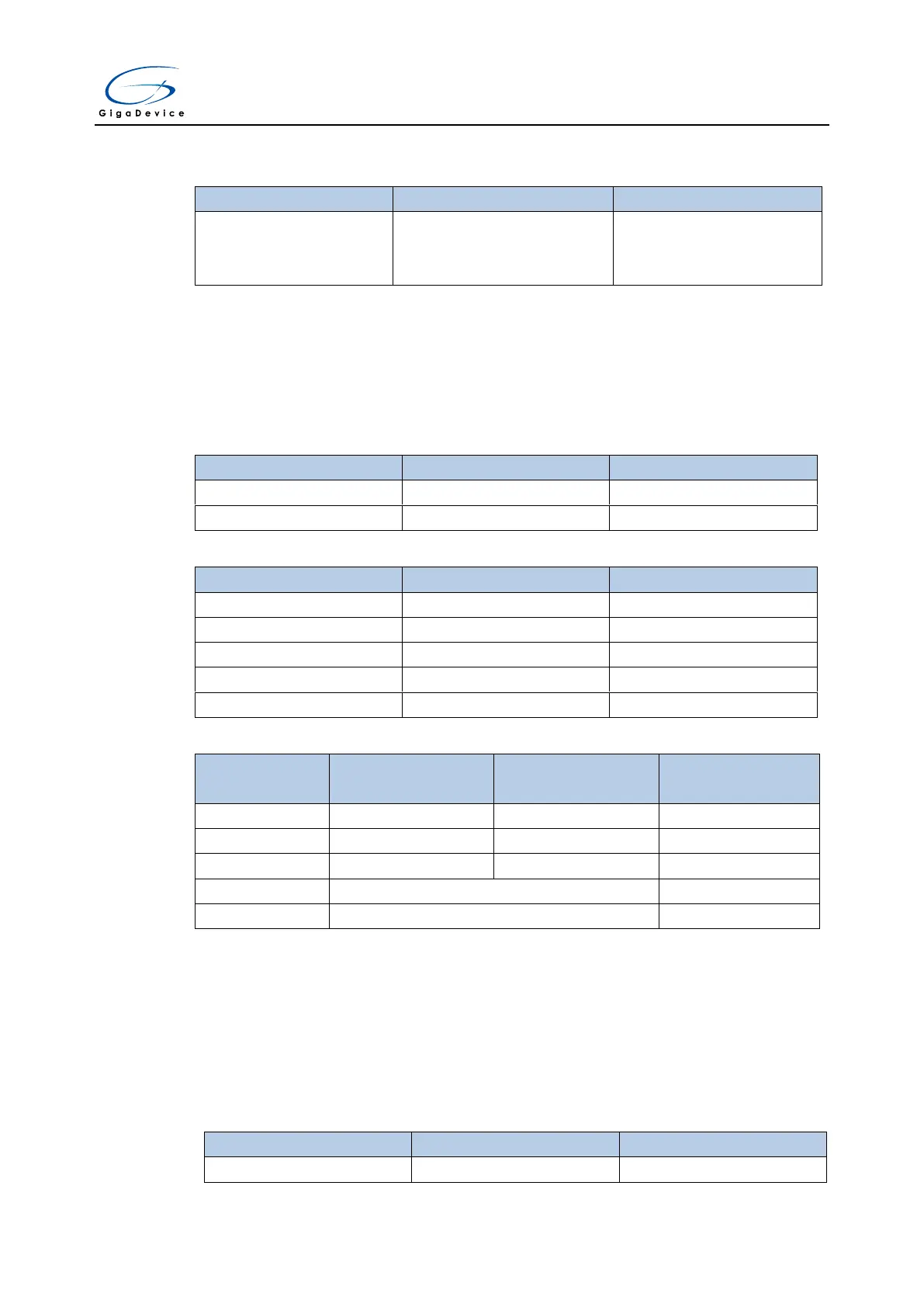
Table 7.8. TIMER4 alternate function remapping
Alternate function
TIMER4CH3_REMAP = 0
TIMER4CH3_REMAP = 1
TIMER4_CH3
TIMER4_CH3 is connected to PA3
IRC40K internal clock is
connected to TIMER4_CH3
input for calibration purpose
1. For different packages and flash sizes please refer to the datasheet.
7.4.5. USART AF remapping
Refer to AFIO port configuration register 0 (AFIO_PCF0).
Table 7.9. USART0 alternate function remapping
Alternate function
USART0_REMAP = 0
USART0_REMAP = 1
USART0_TX
PA9
PB6
USART0_RX
PA10
PB7
Table 7.10. USART1 alternate function remapping
Alternate function
USART1_REMAP = 0
USART1_REMAP = 1
(2)
USART1_CTS
PA0
PD3
USART1_RTS
PA1
PD4
USART1_TX
PA2
PD5
USART1_RX
PA3
PD6
USART1_CK
PA4
PD7
Table 7.11. USART2 alternate function remapping
Alternate function
USART2_REMAP [1:0] =
“00” (no remap)
USART2_REMAP [1:0]
=“01” (partial remap)
(1)
USART2_REMAP [1:0]
=“11” (full remap)
(2)
USART2_TX
PB10
PC10
PD8
USART2_RX
PB11
PC11
PD9
USART2_CK
PB12
PC12
PD10
USART2_CTS
PB13
PD11
USART2_RTS
PB14
PD12
2. Remap available only for 64-pin,100-pin
3. Remap available only 100-pin
7.4.6. I2C0 AF remapping
Refer to AFIO port configuration register 0 (AFIO_ PCF0).
Table 7.12. I2C0 alternate function remapping
Alternate function
I2C0_REMAP = 0
I2C0_REMAP = 1
(1)
I2C0_SCL
PB6
PB8

Table of Contents

Related product manuals