GD32VF103 User Manual
112
7.4.11. CLK pins AF remapping
The LXTAL oscillator pins OSC32_IN and OSC32_OUT can be used as general-purpose I/O
PC14 and PC15 individually, when the LXTAL oscillator is off. The LXTAL has priority over the
GPIOs function.
Note: 1. But when the 1.8 V domain is powered off (by entering standby mode) or when the
backup domain is supplied by V
BAT
(V
DD
no more supplied), the PC14/PC15 GPIO
functionality is lost and will be set in analog mode.
2. Refer to the note on IO usage restrictions in Section Battery backup domain.
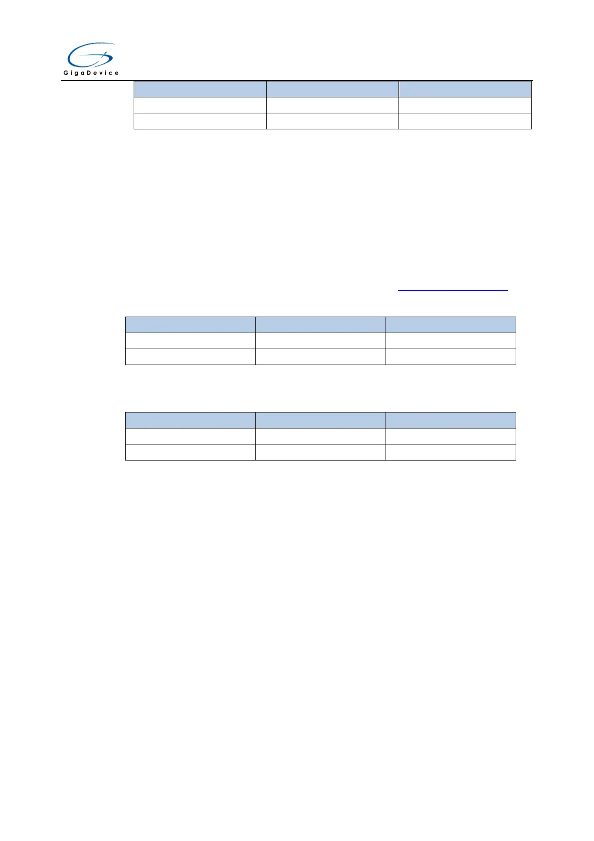
Table 7.17. OSC32 pins configuration
The HXTAL oscillator pins OSC_IN/OSC_OUT can be used as general-purpose I/O PD0/PD1.
Table 7.18. OSC pins configuration

 Loading...
