GD32VF103 User Manual
189
pins gives the pin description.
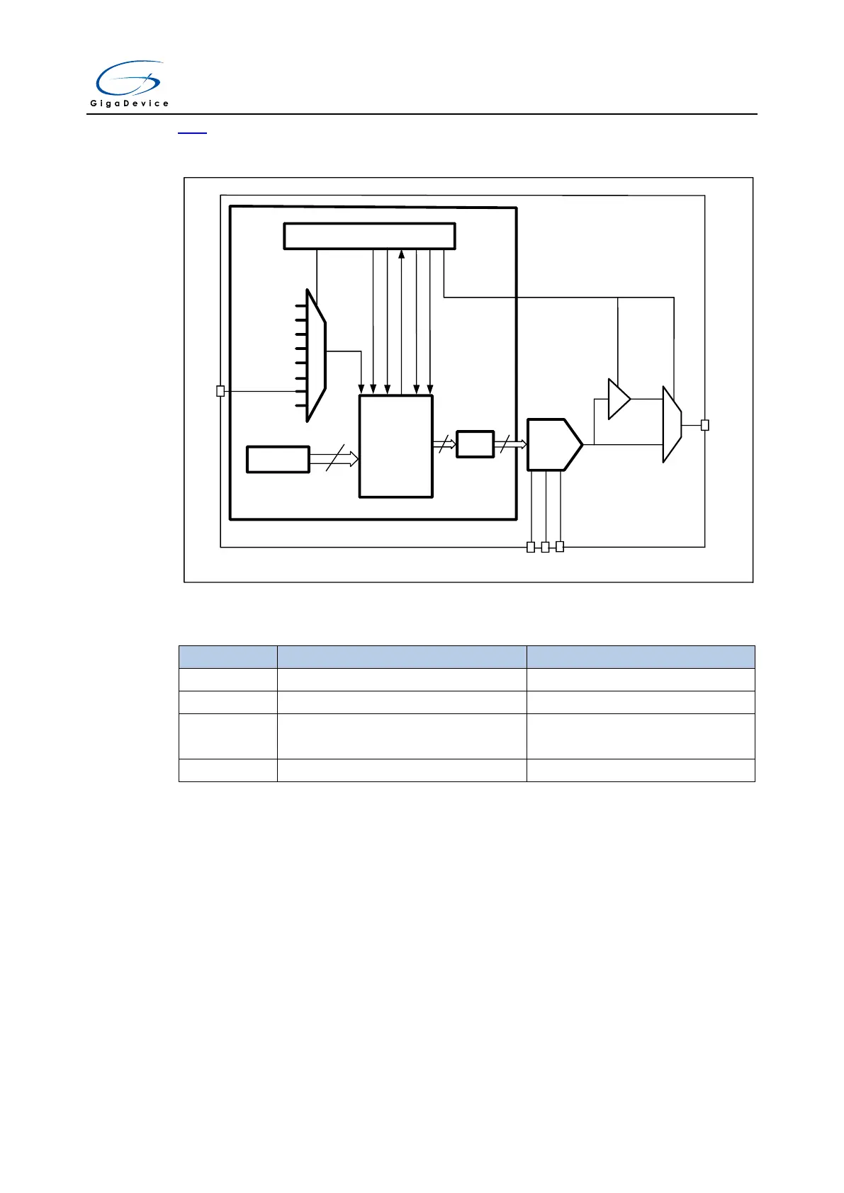
Figure 12-1. DAC block diagram
SWTRx
TIMER5_TRGO
TIMER1_TRGO
Trigger selectorx
DAC control register
DTSELx[2:0]
DMA requestx
DTENx
DHx
12-bit
DOx
12-bit
DAC
Control
logic
VDDA
VSSA
DBOFFx
Buff
MUX2X1
DDMA ENx
DAC_OUTx
12-bit
EXTI9
TIMER7_TRGO
TIMER3_TRGO
VREF+
TIMER6_TRGO
TIMER4_TRGO
DWBWx[3:0]
DWMx[1:0]
Table 12-1. DAC pins
Ground for analog power supply
Input, analog supply ground
Positive reference voltage for the DAC,
Input, analog positive reference
The GPIO pins (PA4 for DAC0, PA5 for DAC1) should be configured to analog mode before
enable the DAC module.
12.3. Function overview
12.3.1. DAC enable
The DACs can be powered on by setting the DENx bit in the DAC_CTL register. A t
WAKEUP
time is needed to startup the analog DAC submodule.



 To Next Page