GD32VF103 User Manual
349
Software can set this bit to send a break frame.
Hardware clears this bit automatically when the break frame has been transmitted.
0: Do not transmit a break frame
1: Transmit a break frame
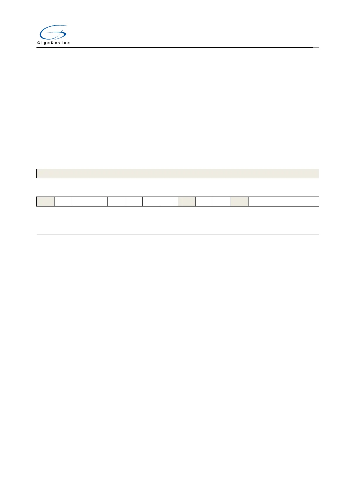
16.4.5. Control register 1 (USART_CTL1)
Address offset: 0x10
Reset value: 0x0000 0000
This register has to be accessed by word (32-bit)
Must be kept the reset value
0: LIN mode disabled
1: LIN mode enabled
This bit field cannot be written when the USART is enabled (UEN=1).
00: 1 stop bit
01: 0.5 stop bit
10: 2 stop bits
11: 1.5 stop bits
This bit field cannot be written when the USART is enabled (UEN=1).
Only 1 stop bit and 2 stop bits are available for UART3/4.
0: CK pin disabled
1: CK pin enabled
This bit field cannot be written when the USART is enabled (UEN=1).
This bit is reserved for UART3/4.
This bit specifies the polarity of the CK pin in synchronous mode.
0: The CK pin is in low state when the USART is in idle state
1: The CK pin is in high state when the USART is in idle state



 To Next Page