GD32VF103 User Manual
235
A DMA request or interrupt is generated by setting CHxG directly.
The input capture mode can be also used for pulse width measurement from signals on the
TIMERx_CHx pins. For example, PWM signal connects to CI0 input. Select CI0 as channel 0
capture signals by setting CH0MS to 2’b01 in the channel control register (TIMERx_CHCTL0)
and set capture on rising edge. Select CI0 as channel 1 capture signal by setting CH1MS to
2’b10 in the channel control register (TIMERx_CHCTL0) and set capture on falling edge. The
counter is set to restart mode and is restarted on channel 0 rising edge. Then the
TIMERX_CH0CV can measure the PWM period and the TIMERx_CH1CV can measure the
PWM duty cycle.
Output compare mode
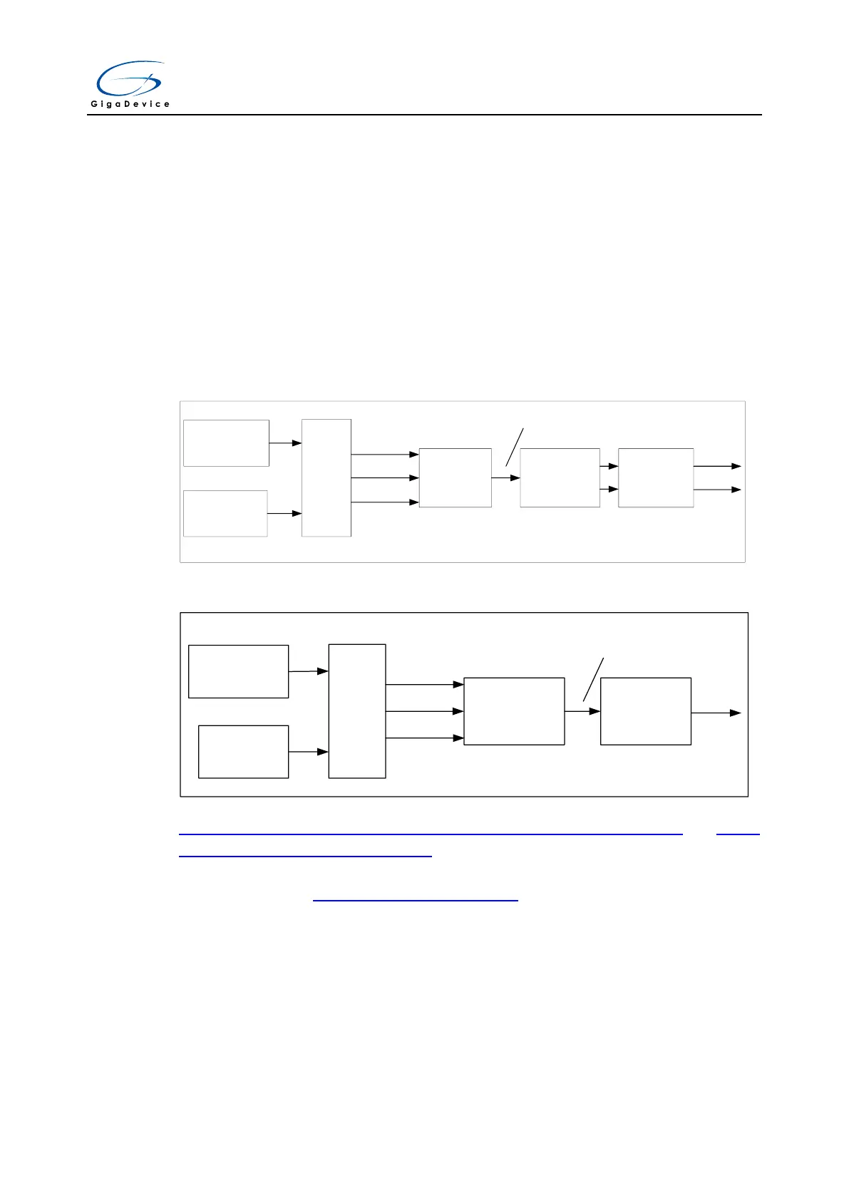
Figure 15-13. Output compare logic (with complementary output, x=0,1,2)
Capture/
compare register
CHxCV
Counter
output comparator
Compare
output control
CHxCOMCTL
CNT>CHxCV
CNT=CHxCV
CNT<CHxCV
Output
complementary
protection
register
&Dead-Time
Output enable
and polarity
selector
CHxP,CHxNP
CHxE,CHxNE
OxCPRE
CHx_O
CHx_ON
Figure 15-14. Output compare logic (CH3_O)
Capture/
compare register
CH3CV
Counter
output comparator
Compare output
control
CH3COMCTL
Output enable
and polarity
selector
CH3P,CH3E
O3CPRE
CH3_O
CNT>CH3CV
CNT=CH3CV
CNT<CH3CV
Figure 15-13. Output compare logic (with complementary output, x=0,1,2) and Figure
15-14. Output compare logic (CH3_O) show the logic circuit of output compare mode. The
relationship between the channel output signal CHx_O/CHx_ON and the OxCPRE signal
(more details refer to Channel output prepare signal) is described as blew: The active level
of O0CPRE is high, the output level of CH0_O/CH0_ON depends on OxCPRE signal,
CHxP/CHxNP bit and CH0E/CH0NE bit (please refer to the TIMERx_CHCTL2 register for
more details). For examples,
1) Configure CHxP=0 (the active level of CHx_O is high, the same as OxCPRE), CHxE=1
(the output of CHx_O is enabled),
If the output of OxCPRE is active(high) level, the output of CHx_O is active(high) level;
If the output of OxCPRE is inactive(low) level, the output of CHx_O is active(low) level.



 To Next Page