GD32VF103 User Manual
477
21.7. Register definition
USBFS base address: 0x5000 0000
21.7.1. Global control and status registers
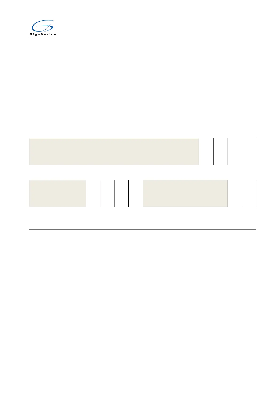
Global OTG control and status register (USBFS_GOTGCS)
Address offset: 0x0000
Reset value: 0x0000 0800
This register has to be accessed by word (32-bit)
Must be kept at reset value
B-Session Valid (described in OTG protocol).
0: Vbus voltage level of a OTG B-Device is below VBSESSVLD
1: Vbus voltage level of a OTG B-Device is above VBSESSVLD
Note: Only accessible in OTG B-Device mode.
A-host mode transceiver status.
0: Vbus voltage level of a OTG A-Device is below VASESSVLD
1: Vbus voltage level of a OTG A-Device is above VASESSVLD
The A-Device is the default host at the start of a session.
Note: Only accessible in OTG A-Device mode.
Debounce interval of a detected connection.
0: Indicates the long debounce interval , when a plug-on and connection occurs on
USB bus
1: Indicates the short debounce interval, when a soft connection is used in HNP