GD32VF103 User Manual
238
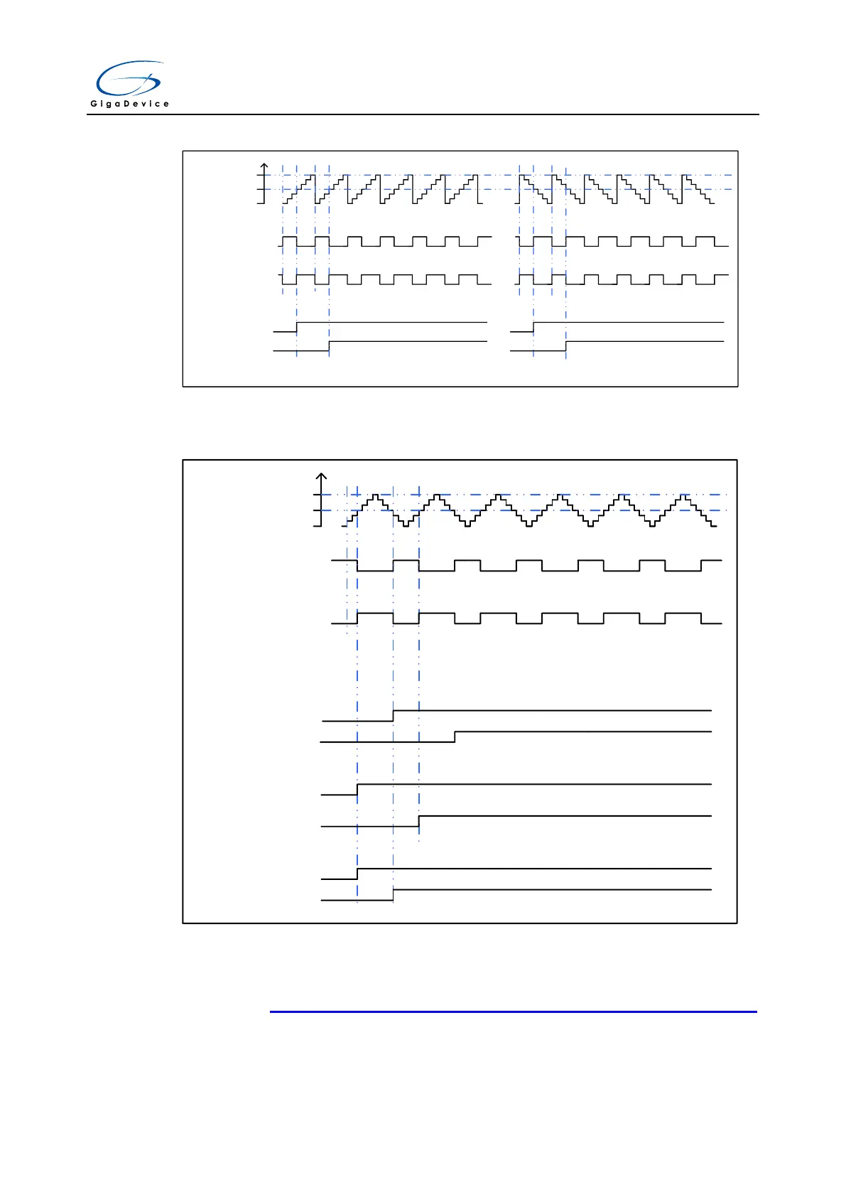
Figure 15-16. Timing chart of EAPWM
0
CHxVAL
CAR
PWM MODE0
PWM MODE1
Cx OUT
Cx OUT
Interrupt signal
CHxIF
CHxOF
Figure 15-17. Timing chart of CAPWM
0
CHxVAL
CAR
PWM MODE0
Cx OUT
PWM MODE1
Cx OUT
Interrupt signal
CHxIF
CHxOF
CAM=2'b01 down only
CAM=2'b10 up only
CHxIF
CHxOF
CAM=2'b11 up/down
CHxIF
CHxOF
Channel output prepare signal
As is shown in Figure 15-13. Output compare logic (with complementary output, x=0,1,2),
when TIMERx is configured in compare match output mode, a middle signal which is OxCPRE
signal (Channel x output prepare signal) will be generated before the channel outputs signal.
The OxCPRE signal type is defined by configuring the CHxCOMCTL bit. The OxCPRE signal



 To Next Page