EasyManua.ls Logo

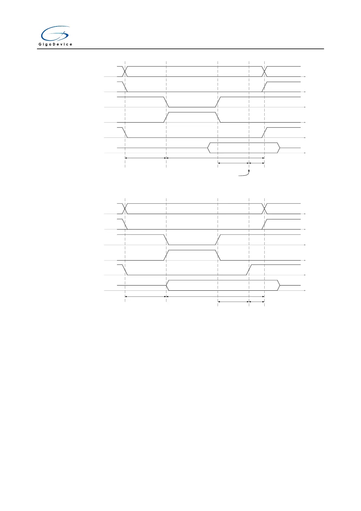
GigaDevice Semiconductor GD32VF103 - Figure 19-7. Write Access Timing Diagram under Async-Wait Signal Assertion; Figure 19-6. Read Access Timing Diagram under Async-Wait Signal Assertion

GigaDevice Semiconductor GD32VF103
536 pages
Print Icon
To Next Page IconTo Next Page
To Previous Page IconTo Previous Page
Loading...
GD32VF103 User Manual
423
Figure 19-6. Read access timing diagram under async-wait signal assertion
Address
(EXMC_A[25:0])
Wait
(EXMC_NWAIT)
NRWTPOL = 0
Chip Enable
(EXMC_NEx)
Output Enable
(EXMC_NOE)
Data
(EXMC_D[15:0])
Address Setup Time Data Setup Time
Memory Output
4 HCLK
Wait
(EXMC_NWAIT)
NRWTPOL = 1
2 HCLK
Data sampling point
Figure 19-7. Write access timing diagram under async-wait signal assertion
Address
(EXMC_A[25:0])
Wait
(EXMC_NWAIT)
NRWTPOL = 0
Chip Enable
(EXMC_NEx)
Write Enable
(EXMC_NWE)
Data
(EXMC_D[15:0])
Address Setup Time Data Setup Time
3 HCLK
EXMC Output
1 HCLK
Wait
(EXMC_NWAIT)
NRWTPOL = 1

Table of Contents