GD32VF103 User Manual
28
0x2002 0000 - 0x2002 FFFF
0x2001 C000 - 0x2001 FFFF
0x2001 8000 - 0x2001 BFFF
0x2000 5000 - 0x2001 7FFF
0x2000 0000 - 0x2000 4FFF
0x1FFF F810 - 0x1FFF FFFF
0x1FFF F800 - 0x1FFF F80F
0x1FFF B000 - 0x1FFF F7FF
0x1FFF 7A10 - 0x1FFF AFFF
0x1FFF 7800 - 0x1FFF 7A0F
0x1FFF 0000 - 0x1FFF 77FF
0x1FFE C010 - 0x1FFE FFFF
0x1FFE C000 - 0x1FFE C00F
0x1001 0000 - 0x1FFE BFFF
0x1000 0000 - 0x1000 FFFF
0x083C 0000 - 0x0FFF FFFF
0x0802 0000 - 0x083B FFFF
0x0800 0000 - 0x0801 FFFF
0x0030 0000 - 0x07FF FFFF
0x0010 0000 - 0x002F FFFF
Aliased to Main
Flash or Boot loader
0x0002 0000 - 0x000F FFFF
0x0000 0000 - 0x0001 FFFF
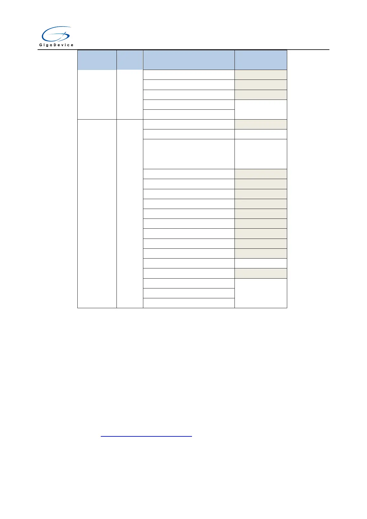
1.3.1. On-chip SRAM memory
The GD32VF103 series of devices contain up to 32 KB of on-chip SRAM which address starts
at 0x2000 0000. It supports byte, half-word (16 bits), and word (32 bits) accesses.
1.3.2. On-chip flash memory overview
The devices provide high density on-chip flash memory, which is organized as follows:
Up to 128KB of main flash memory.
Up to 18KB of information blocks for the boot loader.
Option bytes to configure the device.
Refer to Flash memory controller (FMC) Chapter for more details.