GD32VF103 User Manual
252
3. Configure the TIMER2 in Master/Slave mode by writing MSM=1 (TIMER2_SMCFG
register).
4. Configure TIMER0 to get the input trigger from TIMER2 (TRGS=3’b010 in the
TIMER0_SMCFG register).
5. Configure TIMER0 in event mode (SMC=3’b110 in the TIMER0_SMCFG register).
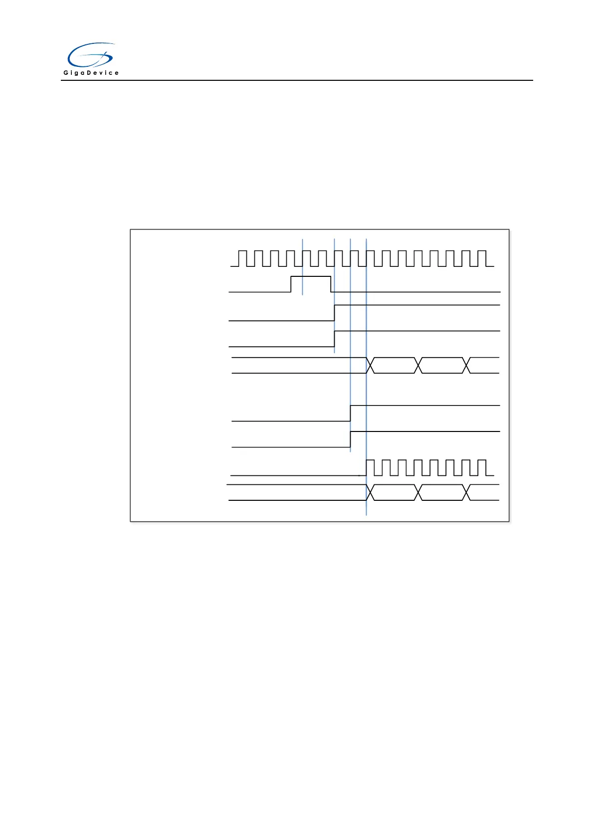
When a rising edge occurs on TIMER2’s CI0, two timer’s counters start counting
synchronously on the internal clock and both TRGIF flags are set.
Figure 15-33. Triggering TIMER0 and TIMER2 with TIMER2’s CI0 input
TIMER_CK
CNT_REG
CNT_REG
CI0
00
01
CEN
02
03
00
01 02
03
CNT_CK
TRGIF
CEN
TRGIF
TIMER2
TIMER0
Timer DMA mode
Timer DMA mode is the function that configures timer’s register by DMA module. The relative
registers are TIMERx_DMACFG and TIMERx_DMATB. Corresponding DMA request bit
should be asserted to enable DMA request for internal interrupt event. TIMERx will send a
request to DMA when the interrupt event occurs. DMA is configured to M2P (memory to
peripheral) mode and the address of TIMERx_DMATB is configured to PADDR (peripheral
base address), then DMA will access the TIMERx_DMATB. In fact, TIMERx_DMATB register
is only a buffer, timer will map the TIMERx_DMATB to an internal register, appointed by the
field of DMATA in TIMERx_DMACFG. If the field of DMATC in TIMERx_DMACFG is 0 (1
transfer), the timer sends only one DMA request. While if TIMERx_DMATC is not 0, such as
3 (4 transfers), then timer will send 3 more requests to DMA, and DMA will access timer’s
registers DMATA+0x4, DMATA+0x8 and DMATA+0xC at the next 3 accesses to
TIMERx_DMATB. In a word, one-time DMA internal interrupt event asserts, (DMATC+1) times

 Loading...
