GD32VF103 User Manual
35
registers.
Wait until all the operations have been finished by checking the value of the BUSY bit in
FMC_STAT registers.
Read and verify the flash memory if required using a DBUS access.
When the operation is executed successfully, the ENDF in FMC_STAT registers is set, and
an interrupt will be triggered by FMC if the ENDIE bit in the FMC_CTL registers is set. Since
all flash data will be modified to a value of 0xFFFF_FFFF, the mass erase operation can be
implemented using a program that runs in SRAM or by using the debugging tool that accesses
the FMC registers directly.
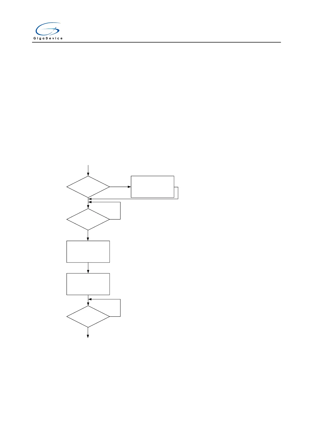
The following figure indicates the mass erase operation flow.
Figure 2-2. Process of mass erase operation
Set the MER bit
Is the LK bit is 0
Send the command
to FMC by setting
START bit
Start
Yes
No
Unlock the
FMC_CTL
Is the BUSY bit is 0
Yes
No
Is the BUSY bit is 0
Yes
No
Finish
2.3.6. Main flash programming
The FMC provides a 32-bit word/16-bit half word programming function which is used to
modify the main flash memory contents. The following steps show the register access
sequence of the word programming operation.