GD32VF103 User Manual
290
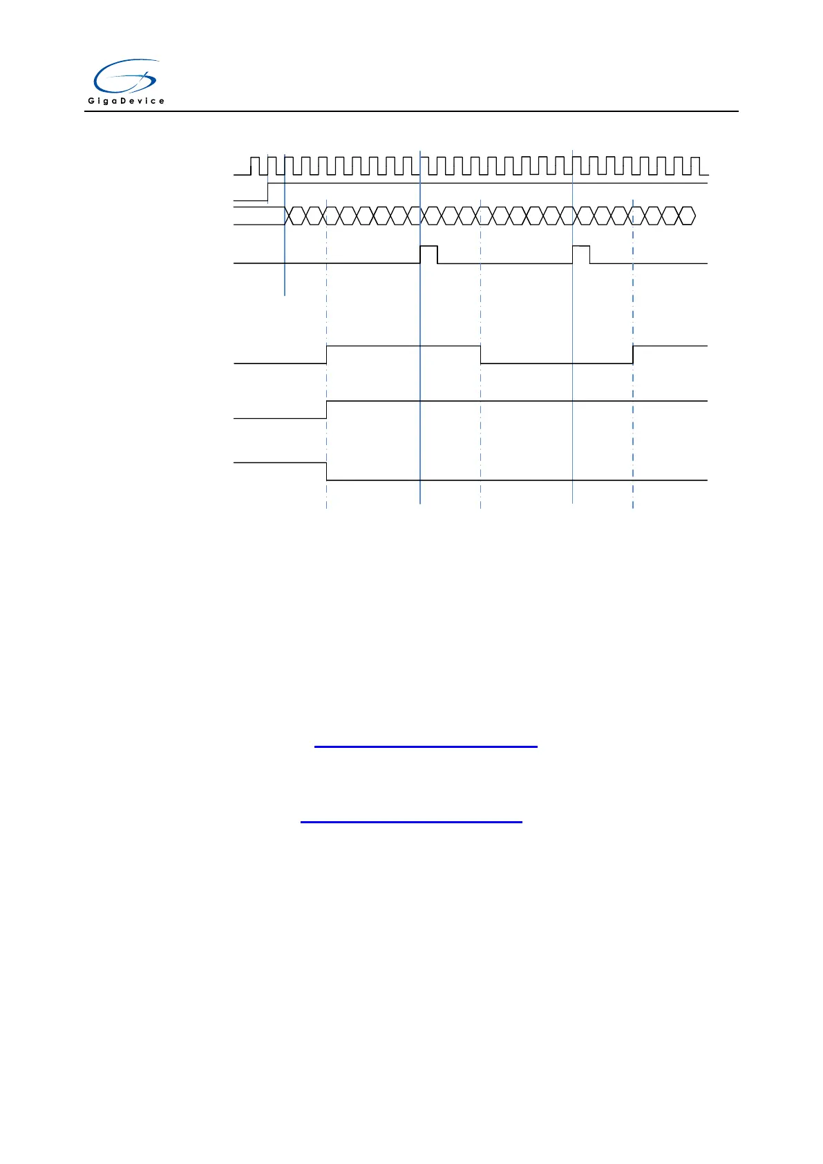
Figure 15-43. Output-compare in three modes
CEN
CNT_REG
00 01 02 03 04 05
….
62 63
Overflow
match toggle
CNT_CLK
OxCPRE
00 01 02 03 04 05
….
62 63
01 02 03 04 05
….
00
match set
match clear
OxCPRE
OxCPRE
PWM mode
In the PWM output mode (by setting the CHxCOMCTL bit to 3’b110 (PWM mode 0) or to 3’b
111(PWM mode 1)), the channel can generate PWM waveform according to the
TIMERx_CAR registers and TIMERx_CHxCV registers.
Based on the counter mode, PWM can also be divided into EAPWM (Edge-aligned PWM)
and CAPWM (Center-aligned PWM).
The EAPWM’s period is determined by TIMERx_CAR and the duty cycle is determined
by TIMERx_CHxCV. Figure 15-44. EAPWM timechart shows the EAPWM output and
interrupts waveform.
The CAPWM period is determined by 2*TIMERx_CAR, and duty cycle is determined by
2*TIMERx_CHxCV. Figure 15-45. CAPWM timechart shows the CAPWM output and
interrupts waveform.
If TIMERx_CHxCV is greater than TIMERx_CAR, the output will be always active under PWM
mode0 (CHxCOMCTL==3’b110).
And if TIMERx_CHxCV is equal to zero, the output will be always inactive under PWM mode0
(CHxCOMCTL==3’b110).

 Loading...
