GD32VF103 User Manual
441
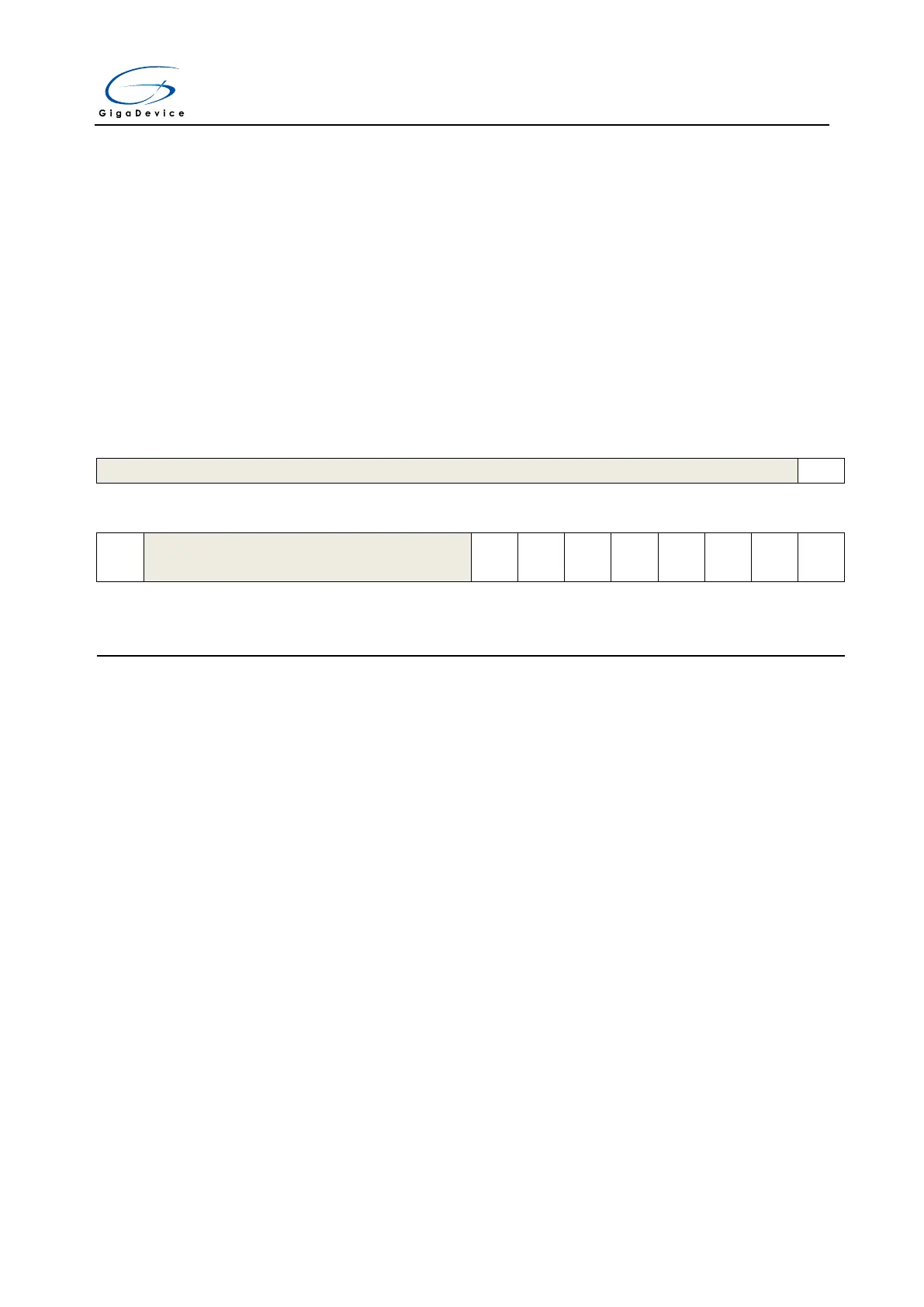
20.4. Register definition
CAN0 base address: 0x4000 6400
CAN1 base address: 0x4000 6800
20.4.1. Control register (CAN_CTL)
Address offset: 0x00
Reset value: 0x0001 0002
This register has to be accessed by word(32-bit)
Must be kept at reset value
If the CANx_HOLD in DBG_CTL register is set, this bit define the CAN stop for
debug or work normal. If the CANx_HOLD in DBG_CTL register is clear, this bit take
not effect.
0: CAN reception and transmission working normal even during debug
1: CAN reception and transmission stop working during debug
0: No effect
1: Reset CAN with working mode of sleep. This bit is automatically reset to 0
Must be kept at reset value
Time-triggered communication
0: Disable time-triggered communication
1: Enable time-triggered communication
Automatic bus-off recovery
0: The bus-off state is left manually by software
1: The bus-off state is left automatically by hardware
If this bit is set, the sleep mode left when CAN bus activity detected, and