GD32VF103 User Manual
210
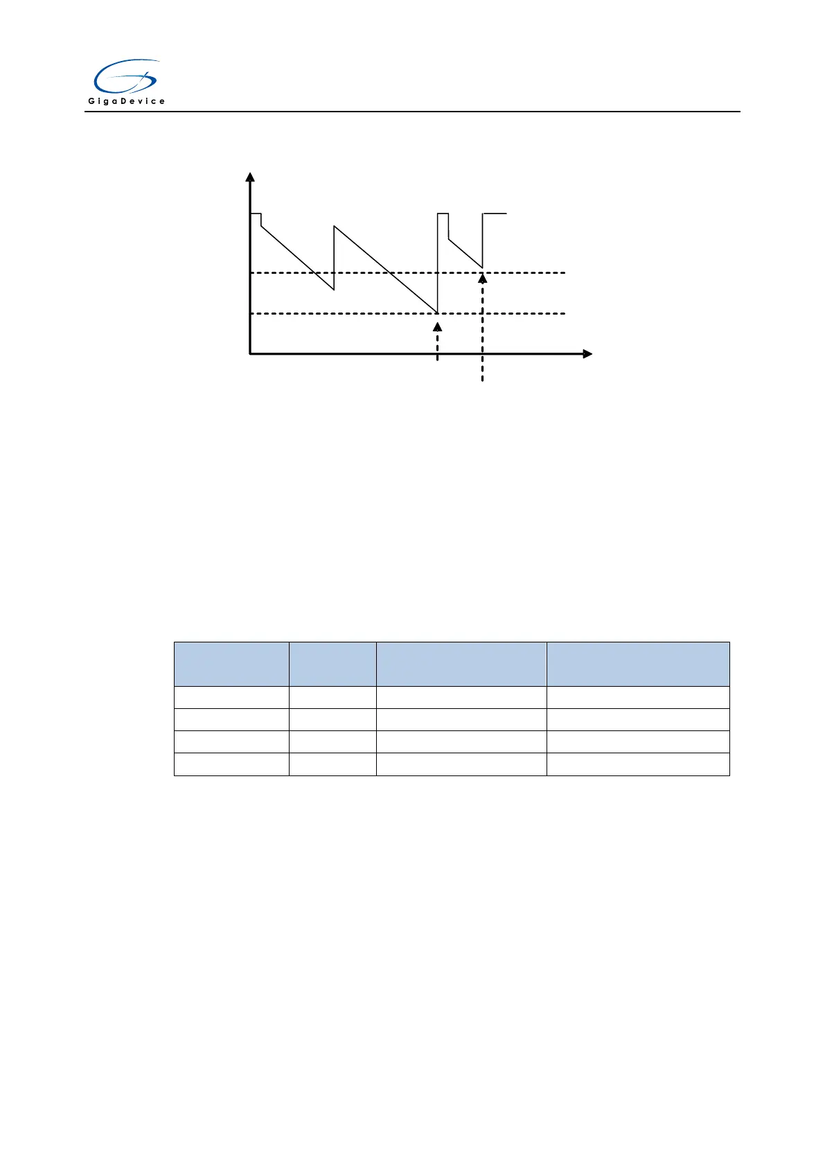
Figure 13.3. Window watchdog timing diagram
Write WWDG_CTL when CTN>WIN
cause a reset
CNT[6]=0 cause a reset
0x7F
Start
CNT[6:0]
0x3F
WIN
Write CNT
Start
Calculate the WWDGT timeout by using the formula below.
t
WWDGT
=t
PCLK1
×4096 ×2
PSC
×
CNT
5:0
+1
(ms (13-1)
where:
t
WWDGT
: WWDGT timeout
t
PCLK1
: APB1 clock period measured in ms
Refer to the table below for the minimum and maximum values of the t
WWDGT
.
Table 13.2. Min/max timeout value at 54 MHz (f
PCLK1
)
If the WWDGT_HOLD bit in DBG module is cleared, the WWDGT continues to work even the
RISC-V core halted (Debug mode). While the WWDGT_HOLD bit is set, the WWDGT stops
in Debug mode.

 Loading...
