GD32VF103 User Manual
248
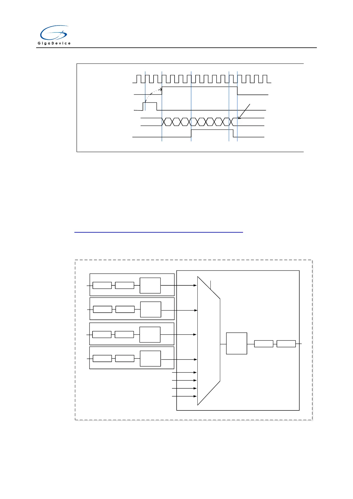
Figure 15-27. Single pulse mode TIMERx_CHxCV=0x04, TIMERx_CAR=0x60
TIMER_CK(CNT_CLK)
CEN
CNT_REG
00 01 02 03 04 05
….
5F 60
00
O2CPRE
CI3
Under SPM, counter stop
Timers interconnection
The timers can be internally connected together for timer chaining or synchronization. This
can be implemented by configuring one timer to operate in the master mode while configuring
another timer to be in the slave mode. The following figures present several examples of
trigger selection for the master and slave modes.
Figure 15-28. TIMER0 Master/Slave mode timer example shows the timer0 trigger
selection when it is configured in slave mode.
Figure 15-28. TIMER0 Master/Slave mode timer example
TIMER0
TIMER 4
Prescaler Counter
Master
mode
control
Trigger
selection
ITI0
IT1
ITI1
CI0F_ED
CI0FE0
CI1FE1
ETIFP
TRGS
Slave mode
control
Prescaler Counter
TRGO
TIMER 1
Prescaler Counter
Master
mode
control
TRGO
TIMER 2
Prescaler Counter
Master
mode
control
ITI2
IT1
ITI3
TRGO
TIMER 3
Prescaler Counter
Master
mode
control
TRGO
Other interconnection examples:
TIMER2 as prescaler for TIMER0



 To Next Page