GD32VF103 User Manual
355
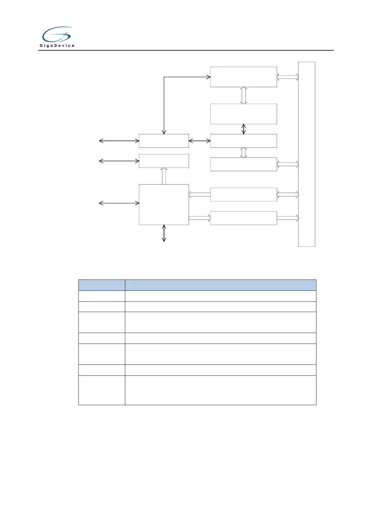
Figure 17-1. I2C module block diagram
Data Register
APB Bus
Shift RegisterSDA Controller
CRC Calculation /
Check
PEC register
SCL Controller
Timing and
Control Logic
Control Registers
Status Flags
SDA
SCL
SMBA
DMA/ Interrupts
Table 17-1. Definition of I2C-bus terminology (refer to the I2C specification of philips
semiconductors)
the device which sends data to the bus
the device which receives data from the bus
the device which initiates a transfer, generates clock signal and terminates
a transfer
the device addressed by a master
more than one master can attempt to control the bus at the same time
without corrupting the message
procedure to synchronize the clock signal of two or more devices
procedure to ensure that, if more than one master tries to control the bus
simultaneously, only one is allowed to do so and the winning master’s
message is not corrupted
17.3.1. SDA and SCL lines
The I2C module has two external lines, the serial data SDA and serial clock SCL lines. The
two wires carry information between the devices connected to the bus.
Both SDA and SCL are bidirectional lines, connected to a positive supply voltage via current-
source or p ull-up resistor. When the bus is free, both lines are HIGH. The output stages of