GD32VF103 User Manual
413
The hardware computes the CRC value after each transmitted bit, when the TRANS
is set, a read to this register could return an intermediate value. The different frame
formats (LF bit of the SPI_CTL0) will get different CRC values.
This register is reset when the CRCEN bit in SPI_CTL0 register or the SPIxRST bit
in RCU reset register is set.
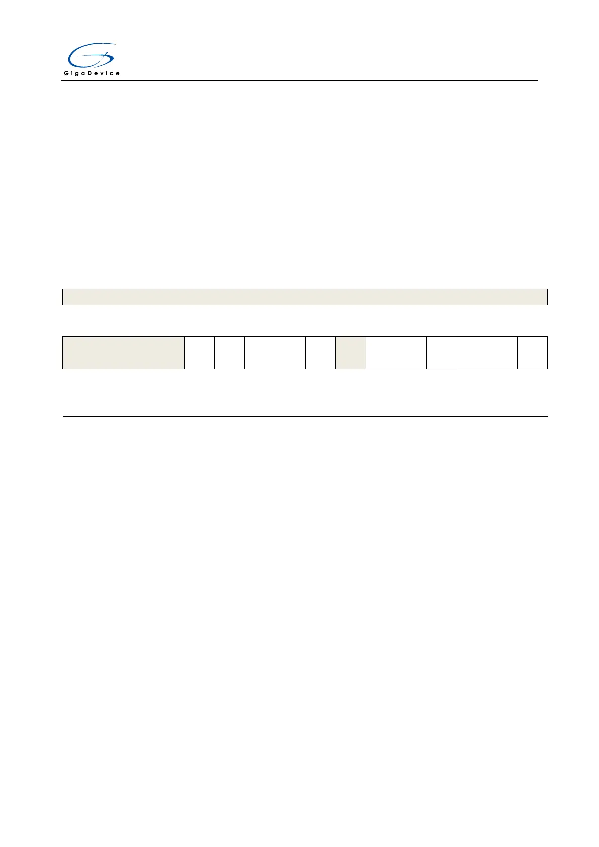
18.11.8. I2S control register (SPI_I2SCTL)
Address offset: 0x1C
Reset value: 0x0000
This register can be accessed by half-word (16-bit) or word (32-bit).
Must be kept at reset value.
0: SPI mode
1: I2S mode
This bit should be configured when SPI/I2S is disabled.
0: I2S is disabled
1: I2S is enabled
This bit is not used in SPI mode.
00: Slave transmission mode
01: Slave reception mode
10: Master transmission mode
11: Master reception mode
This bit should be configured when I2S is disabled.
This bit is not used in SPI mode.
PCM frame synchronization mode
0: Short frame synchronization
1: Long frame synchronization
This bit has a meaning only when PCM standard is used.