GD32VF103 User Manual
397
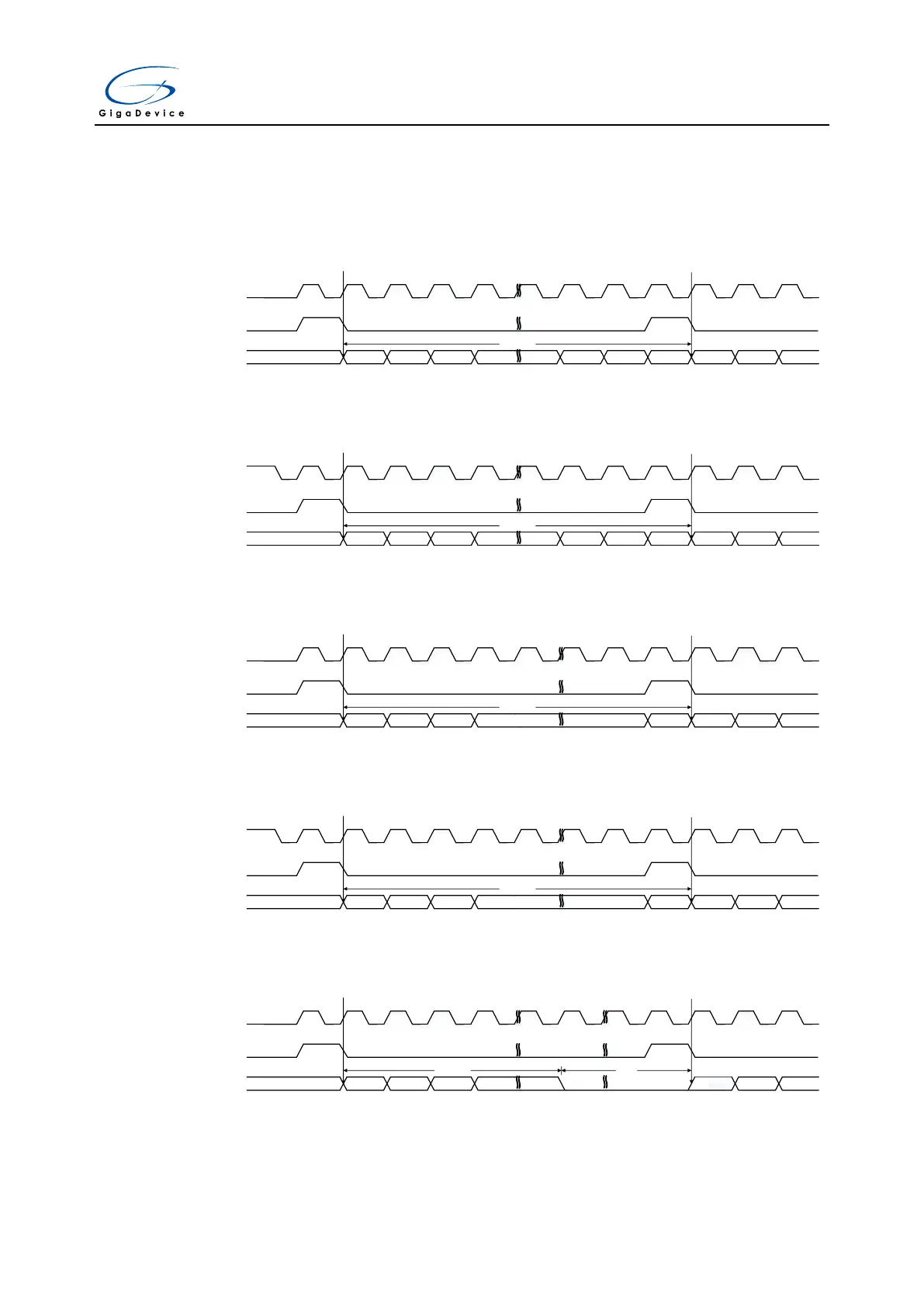
configurable using the PCMSMOD bit in the SPI_I2SCTL register. The SPI_DATA register is
handled in the exactly same way as that for I2S Phillips standard. The timing diagrams for
each configuration of the short frame synchronization mode are shown below.
Figure 18-32. PCM standard short frame synchronization mode timing diagram
(DTLEN=00, CHLEN=0, CKPL=0)
I2S_CK
I2S_SD
16-bit data
MSB
I2S_WS
MSB LSB
frame 1 frame 2
Figure 18-33. PCM standard short frame synchronization mode timing diagram
(DTLEN=00, CHLEN=0, CKPL=1)
I2S_CK
I2S_SD
16-bit data
MSB
I2S_WS
MSB LSB
frame 1 frame 2
Figure 18-34. PCM standard short frame synchronization mode timing diagram
(DTLEN=10, CHLEN=1, CKPL=0)
I2S_CK
I2S_SD
32-bit data
MSB
I2S_WS
MSB LSB
frame 1 frame 2
Figure 18-35. PCM standard short frame synchronization mode timing diagram
(DTLEN=10, CHLEN=1, CKPL=1)
I2S_CK
I2S_SD
32-bit data
MSB
I2S_WS
MSB LSB
frame 1 frame 2
Figure 18-36. PCM standard short frame synchronization mode timing diagram
(DTLEN=01, CHLEN=1, CKPL=0)
I2S_CK
I2S_SD
24-bit data
MSB
I2S_WS
MSB
frame 1 frame 2
8-bit 0
Figure 18-37. PCM standard short frame synchronization mode timing diagram