GD32VF103 User Manual
424
19.4. Register definition
EXMC base address: 0xA000 0000
19.4.1. NOR/PSRAM controller registers
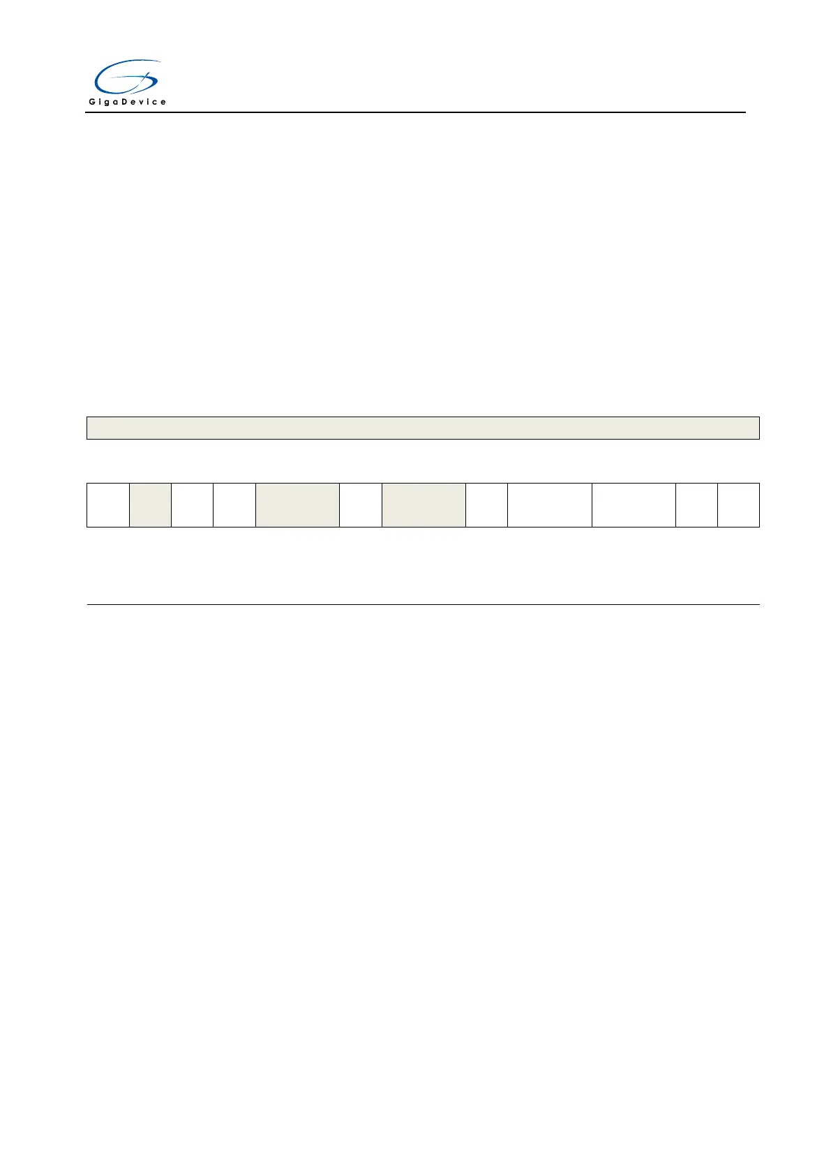
SRAM/NOR Flash control registers (EXMC_SNCTLx) (x=0)
Address offset: 0x00 + 8 * x, (x = 0)
Reset value: 0x0000 30DA for region0.
This register has to be accessed by word (32-bit)
Must be kept at reset value.
0: Disable the asynchronous wait feature
1: Enable the asynchronous wait feature
Must be kept at reset value.
For Flash memory access in burst mode, this bit enables/disables wait-state
insertion via the NWAIT signal:
0: Disable NWAIT signal
1: Enable NWAIT signal
0: Disabled write in the bank by the EXMC, otherwise an AHB error is reported
1: Enabled write in the bank by the EXMC (default after reset)
Must be kept at reset value.
0: Low level is active of NWAIT
1: High level is active of NWAIT

 Loading...
