GD32VF103 User Manual
103
General purpose
Output (GPIO)
01: Speed up to 10MHz
10: Speed up to 2MHz
11: Speed up to 50MHz
Alternate Function
Output (AFIO)
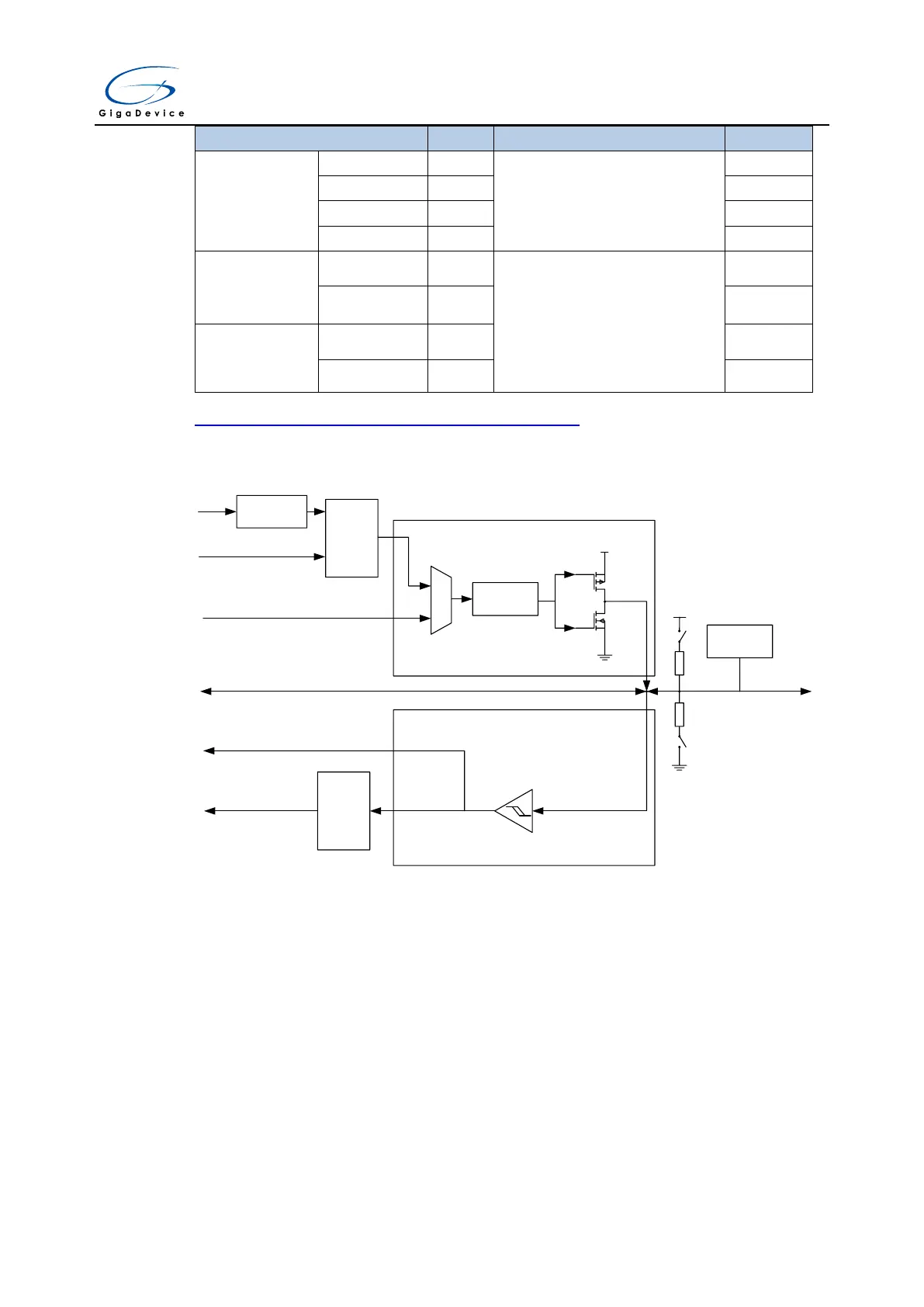
Figure 7.1. Basic structure of a standard I/O port bit shows the basic structure of an I/O
port bit.
Figure 7.1. Basic structure of a standard I/O port bit
Vss
Output
Control
Vdd
Output
Control
Register
Input
Status
Register
Write
Read/Write
Alternate Function Output
Read
Alternate Function Input
Analog ( Input / Output )
Input driver
Output driver
I/O pin
Schmitt
trigger
Bit Operate
Registers
ESD
protection
Vdd
Vss
7.3.1. GPIO pin configuration
During or just after the reset period, the alternative functions are all inactive and the GPIO
ports are configured into the input floating mode that input disabled without Pull-Up (PU)/Pull-
Down (PD) resistors. But the JTAG/Serial-Wired Debug pins are in input PU/PD mode after
reset:
PA15: JTDI in PU mode.
PA14: JTCK in PD mode.
PA13: JTMS in PU mode.
PB4: NJTRST in PU mode.
PB3: JTDO in Floating mode.

 Loading...
