GD32VF103 User Manual
375
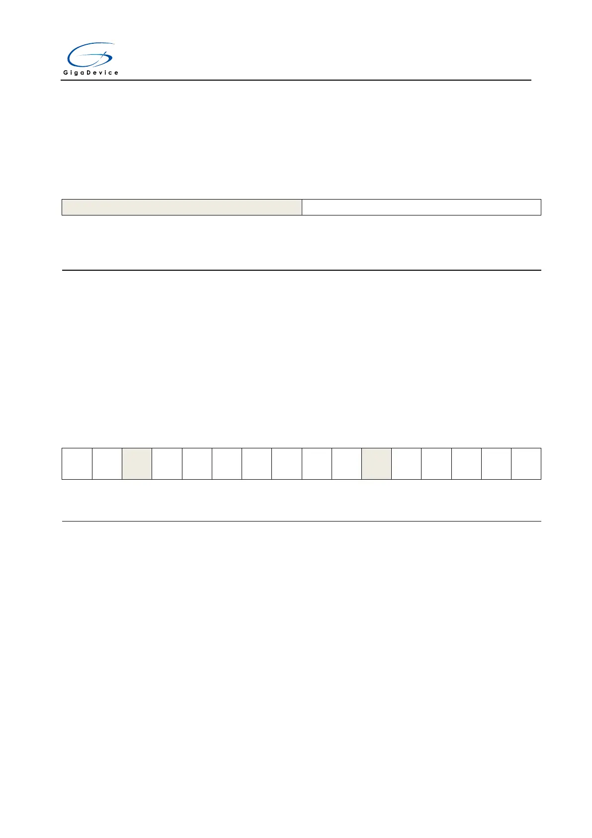
17.4.5. Transfer buffer register (I2C_DATA)
Address offset: 0x10
Reset value: 0x0000
This register can be accessed by half-word (16-bit) or word (32-bit)
Must be kept the reset value.
Transmission or reception data buffer
17.4.6. Transfer status register 0 (I2C_STAT0)
Address offset: 0x14
Reset value: 0x0000
This register can be accessed by half-word (16-bit) or word (32-bit)
This bit is set by hardware and cleared by writing 0.
0: SMBA pin not pulled down (device mode) or no Alert detected (host mode)
1: SMBA pin pulled down (device mode) or Alert detected (host mode)
Timeout signal in SMBus mode
This bit is set by hardware and cleared by writing 0.
0: No timeout error
1: Timeout event occurs (SCL is low for 25 ms)
Must keep the reset value.
PEC error when receiving data
This bit is set by hardware and cleared by writing 0.
0: Received PEC and calculated PEC match
1: Received PEC and calculated PEC don’t match, I2C will send NACK careless of