GD32VF103 User Manual
162
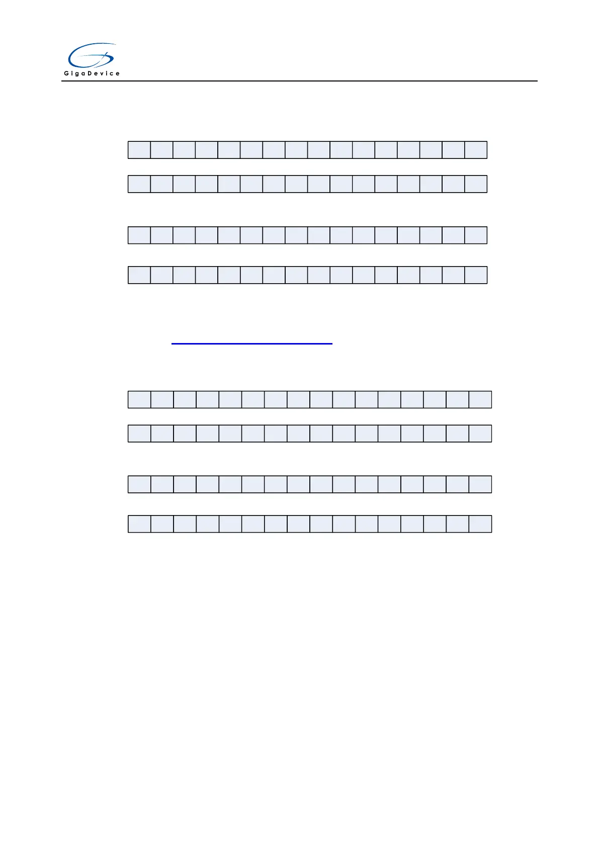
inserted group data value may be a negative value. The sign value is extended.
Figure 11-9. 12-bit Data alignment
Sign Sign Sign Sign D11 D10 D9 D8 D7 D6 D5 D4 D3 D2 D1 D0
0 0 0 0 D11 D10 D9 D8 D7 D6 D5 D4 D3 D2 D1 D0
Regular group data
Inserted group data
0 0 0Sign D11 D10 D9 D8 D7 D6 D5 D4 D3 D2 D1 D0
0 0 0 0D11 D10 D9 D8 D7 D6 D5 D4 D3 D2 D1 D0
Regular group data
Inserted group data
DAL=0
DAL=1
6-bit resolution data alignment is different from 12-bit/10-bit/8-bit resolution data alignment,
shown as Figure 11-10. 6-bit Data alignment .
Figure 11-10. 6-bit Data alignment
Sign Sign Sign Sign Sign Sign Sign Sign Sign Sign D5 D4 D3 D2 D1 D0
0 0 0 0 0 0 0 0 0 0 D5 D4 D3 D2 D1 D0
Regular group data
Inserted group data
D1 D0 0Sign Sign Sign Sign Sign Sign Sign Sign Sign D5 D4 D3 D2
D1 D0 0 00 0 0 0 0 0 0 0 D5 D4 D2
Regular group data
Inserted group data
DAL=0
DAL=1
D3
11.4.8. Programmable sample time
The number of ADCCLK cycles which is used to sample the input voltage can be specified by
the SPTn[2:0] bits in the ADC_SAMPT0 and ADC_SAMPT1 registers. A different sample time
can be specified for each channel. For 12-bits resolution, the total conversion time is
“sampling time + 12.5” ADCCLK cycles.
Example:
ADCCLK = 10MHz and sample time is 1.5 cycles, the total conversion time is “1.5+12.5”
ADCCLK cycles, that means 1.4us.

 Loading...
