GD32VF103 User Manual
396
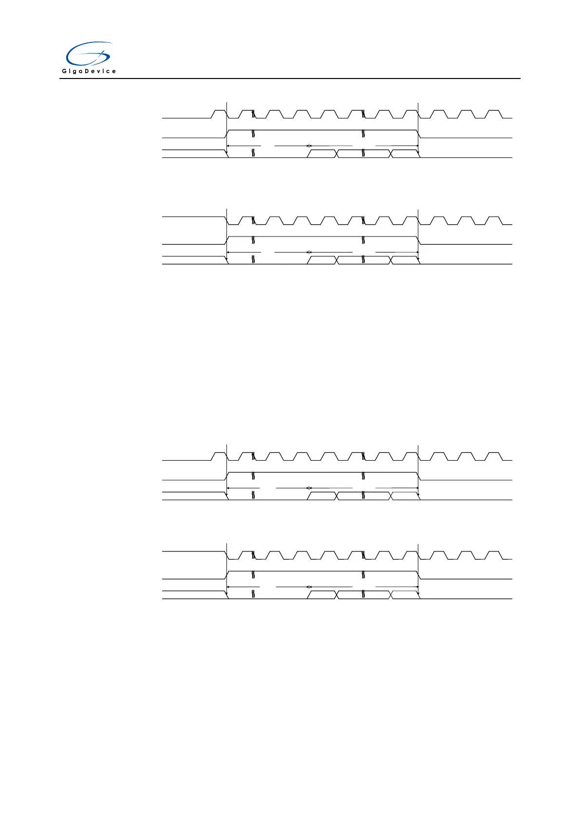
Figure 18-28. LSB justified standard timing diagram (DTLEN=01, CHLEN=1, CKPL=0)
I2S_CK
I2S_SD
8-bit 0
frame 1 (channel left) frame 2 (channel right)
I2S_WS
24-bit data
MSB LSB
Figure 18-29. LSB justified standard timing diagram (DTLEN=01, CHLEN=1, CKPL=1)
I2S_CK
I2S_SD
8-bit 0
frame 1 (channel left) frame 2 (channel right)
I2S_WS
24-bit data
MSB LSB
When the packet type is 24-bit data packed in 32-bit frame, two write or read operations to or
from the SPI_DATA register are needed to complete the transmission of a frame. In
transmission mode, if a 24-bit data D[23:0] is going to be sent, the first data written to the
SPI_DATA register should be a 16-bit data. The higher 8 bits of the 16-bit data can be any
value and the lower 8 bits should be D[23:16]. The second data written to the SPI_DATA
register should be D[15:0]. In reception mode, if a 24-bit data D[23:0] is received, the first data
read from the SPI_DATA register is a 16-bit data. The high 8 bits of this 16-bit data are zeros
and the lower 8 bits are D[23:16]. The second data read from the SPI_DATA register is
D[15:0].
Figure 18-30. LSB justified standard timing diagram (DTLEN=00, CHLEN=1, CKPL=0)
I2S_CK
I2S_SD
16-bit 0
frame 1 (channel left) frame 2 (channel right)
I2S_WS
16-bit data
MSB LSB
Figure 18-31. LSB justified standard timing diagram (DTLEN=00, CHLEN=1, CKPL=1)
I2S_CK
I2S_SD
16-bit 0
frame 1 (channel left) frame 2 (channel right)
I2S_WS
16-bit data
MSB LSB
When the packet type is 16-bit data packed in 32-bit frame, only one write or read operation
to or from the SPI_DATA register is needed to complete the transmission of a frame. The
remaining 16 bits are forced by hardware to 0x0000 to extend the data to 32-bit format.
PCM standard
For PCM standard, I2S_WS and I2S_SD are updated on the rising edge of I2S_CK, and the
I2S_WS signal indicates frame synchronization information. Both the short frame
synchronization mode and the long frame synchronization mode are available and


 To Next Page