GD32VF103 User Manual
371
17.4. Register definition
I2C0 base address: 0x4000 5400
I2C1 base address: 0x4000 5800
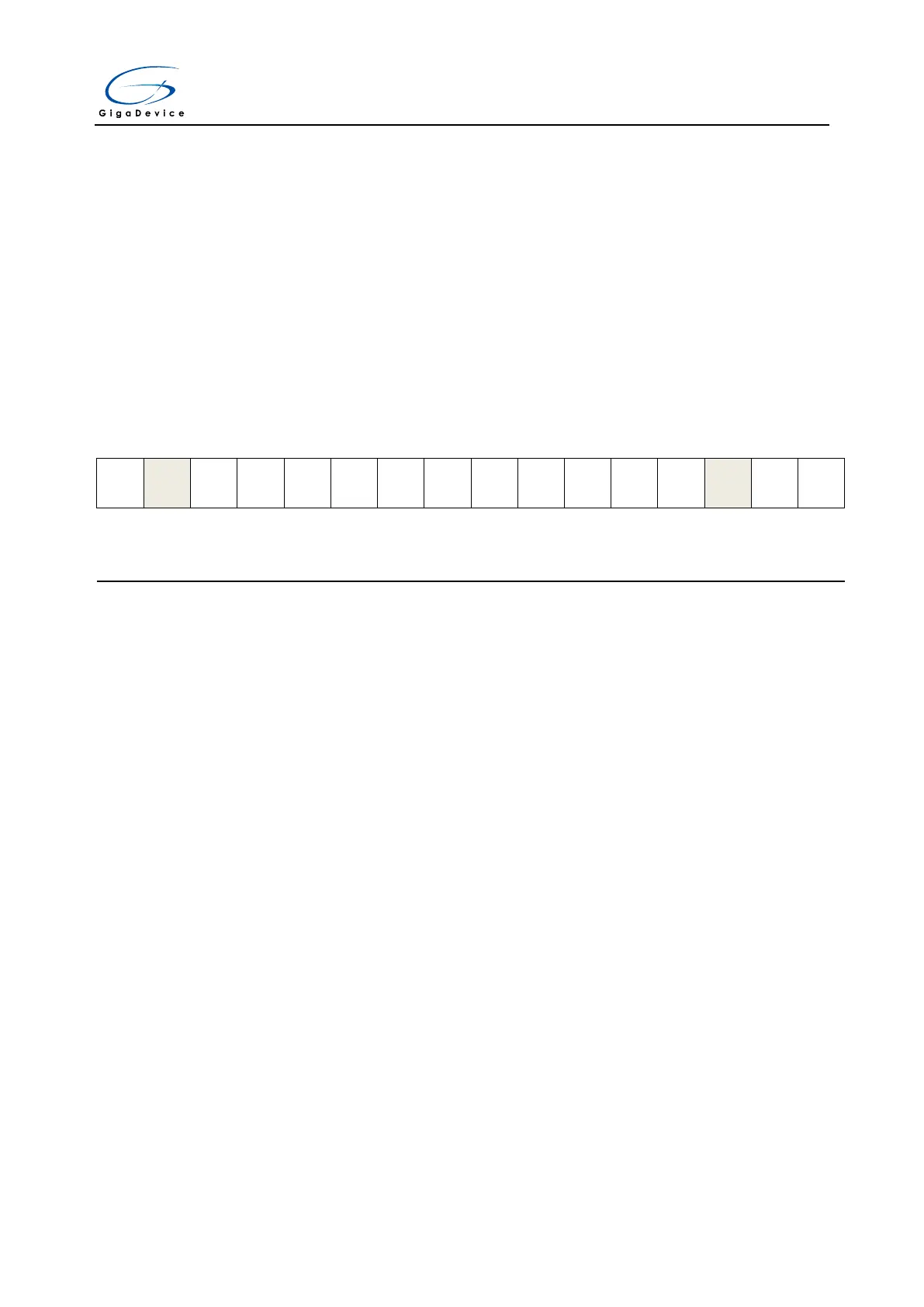
17.4.1. Control register 0 (I2C_CTL0)
Address offset: 0x00
Reset value: 0x0000
This register can be accessed by half-word (16-bit) or word (32-bit)
Software reset I2C, software should wait until the I2C lines are released to reset the
I2C
0: I2C is not under reset
1: I2C is under reset
Must be kept the reset value.
Issue alert through SMBA pin.
Software can set and clear this bit and hardware can clear this bit.
0: Don’t issue alert through SMBA pin
1: Issue alert through SMBA pin
Software set and clear this bit while hardware clears this bit when PEC is transferred
or START/STOP condition detected or I2CEN=0
0: Don’t transfer PEC value
1: Transfer PEC
Position of ACK and PEC when receiving
This bit is set and cleared by software and cleared by hardware when I2CEN=0
0: ACKEN bit specifies whether to send ACK or NACK for the current byte that is
being received. PECTRANS bit indicates that the current receiving byte is a PEC
byte
1: ACKEN bit specifies whether to send ACK or NACK for the next byte that is to be
received, PECTRANS bit indicates the next byte that is to be received is a PEC byte


 To Next Page