Datasheet 177
Functional Description
NOTES:
1. The OCW1 register must be read before entering ALT access mode.
2. Bits 5, 3, 1, and 0 return 0.
08h 6
1 DMA Chan 0–3 Command
2
CAh 2
1
DMA Chan 6 base count low
byte
2 DMA Chan 0–3 Request 2
DMA Chan 6 base count
high byte
3
DMA Chan 0 Mode:
Bits(1:0) = 00
CCh 2
1
DMA Chan 7 base address
low byte
4
DMA Chan 1 Mode:
Bits(1:0) = 01
2
DMA Chan 7 base address
high byte
5
DMA Chan 2 Mode:
Bits(1:0) = 10
CEh 2
1
DMA Chan 7 base count low
byte
6
DMA Chan 3 Mode: Bits(1:0)
= 11.
2
DMA Chan 7 base count
high byte
20h 12
1 PIC ICW2 of Master controller
D0h 6
1 DMA Chan 4–7 Command
2
2 PIC ICW3 of Master controller 2 DMA Chan 4–7 Request
3 PIC ICW4 of Master controller 3
DMA Chan 4 Mode:
Bits(1:0) = 00
4
PIC OCW1 of Master
controller
1
4
DMA Chan 5 Mode:
Bits(1:0) = 01
5
PIC OCW2 of Master
controller
5
DMA Chan 6 Mode:
Bits(1:0) = 10
6
PIC OCW3 of Master
controller
6
DMA Chan 7 Mode:
Bits(1:0) = 11.
7 PIC ICW2 of Slave controller
8 PIC ICW3 of Slave controller
9 PIC ICW4 of Slave controller
10
PIC OCW1 of Slave
controller
1
11 PIC OCW2 of Slave controller
12 PIC OCW3 of Slave controller
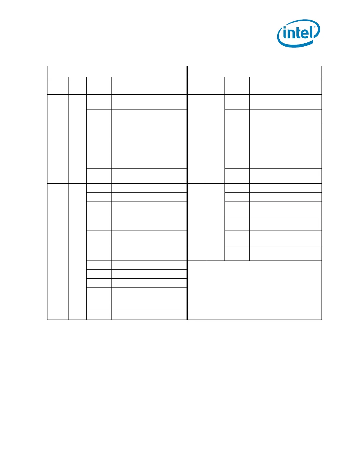
Table 5-36. Write Only Registers with Read Paths in ALT Access Mode (Sheet 2 of 2)
Restore Data Restore Data
I/O
Addr
# of
Rds
Access Data
I/O
Addr
# of
Rds
Access Data

 Loading...