Datasheet 257
Functional Description
5.26.2.1.2 Single Channel versus Dual Channel Mode
In the single channel mode, only Channel-A is used. Channel-B cannot be used for
single channel mode. In the dual channel mode, both Channel-A and Channel-B pins
are used concurrently to drive one LVDS display.
In Single Channel mode, Channel A can take 18 bits of RGB pixel data, plus 3 bits of
timing control (HSYNC/VSYNC/DE) and output them on three differential data pair
outputs; or 24 bits of RGB (plus 4 bits of timing control) output on four differential data
pair outputs. A dual channel interface converts 36 or 48 bits of color information plus
the 3 or 4 bits of timing control respectively and outputs it on six or eight sets of
differential data outputs respectively.
Dual Channel mode uses twice the number of LVDS pairs and transfers the pixel data at
twice the rate of the single channel. In general, one channel will be used for even pixels
and the other for odd pixel data. The first pixel of the line is determined by the display
enable going active and that pixel will be sent out Channel-A. All horizontal timings for
active, sync, and blank will be limited to be on two pixel boundaries in the two channel
modes.
Note: Platforms using the PCH for integrated graphics support 24-bpp display panels of Type
1 only (compatible with VESA LVDS color mapping).
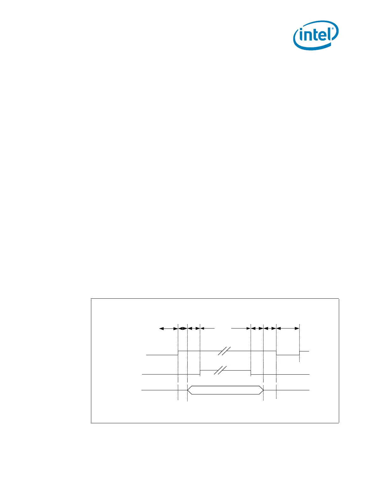
5.26.2.1.3 Panel Power Sequencing
This section provides details for the power sequence timing relationship of the panel
power, the backlight enable and the LVDS data timing delivery. To meet the panel
power timing specification requirements two signals, LFP_VDD_EN and LFP_BKLT_EN,
are provided to control the timing sequencing function of the panel and the backlight
power supplies.
A defined power sequence is recommended when enabling the panel or disabling the
panel. The set of timing parameters can vary from panel to panel vendor, provided that
they stay within a predefined range of values. The panel VDD power, the backlight on/
off state and the LVDS clock and data lines are all managed by an internal power
sequencer.
NOTE: Support for programming parameters TX and T1 through T5 using software is provided.
Figure 5-15. Panel Power Sequencing
Power On Sequence from off state and
Power Off Sequence after full On
Panel VDD
Enable
Panel
BackLight
Enable
Clock/Data Lines
T1+T2
T5 T3
Valid
T4
Panel
On
Off Off
TX
T4
 Loading...
