Datasheet 261
Functional Description
5.26.2.9.1 Control Bus
Communication to SDVO registers and if utilized, ADD2 PROMs and monitor DDCs, are
accomplished by using the SDVOCTRLDATA and SDVOCTRLCLK signals through the
SDVO device. These signals run up to 400 kHz and connect directly to the SDVO
device.
The SDVO device is then responsible for routing the DDC and PROM data streams to
the appropriate location. Consult SDVO device data sheets for level shifting require-
ments of these signals.
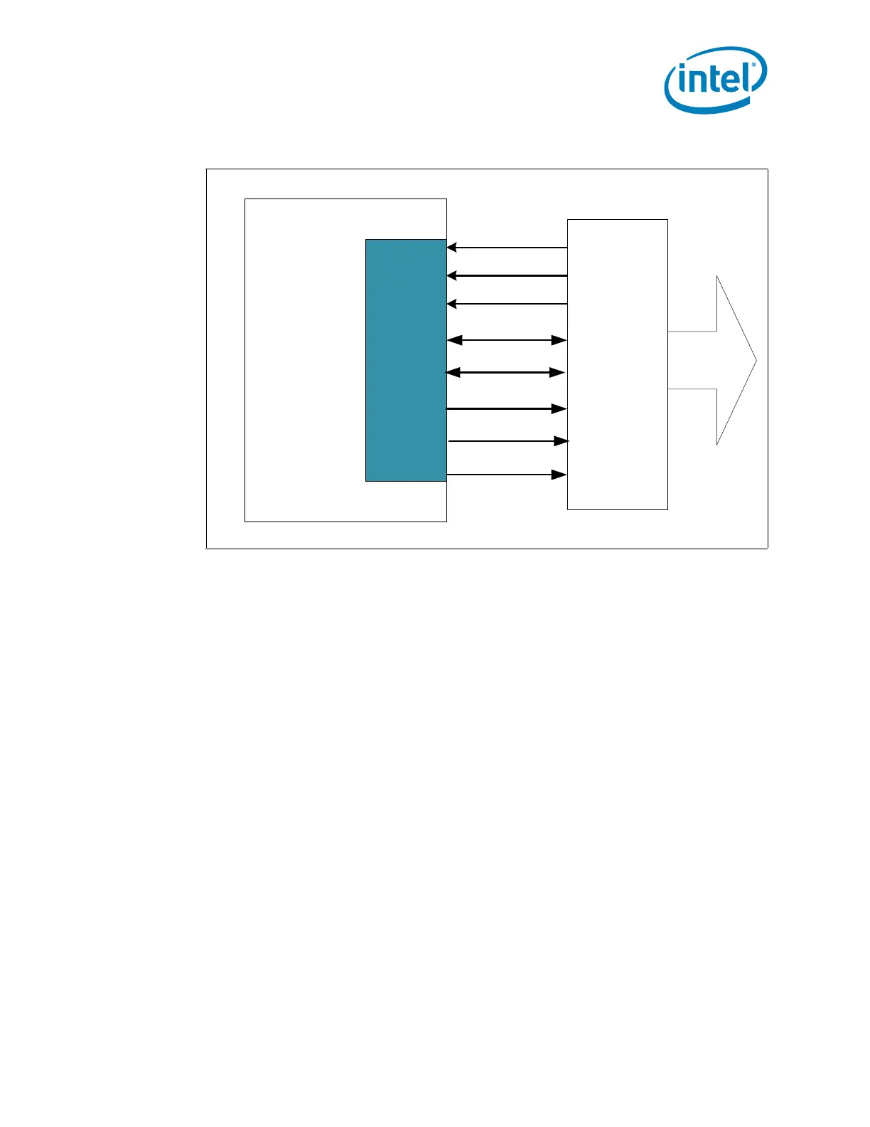
Figure 5-18. SDVO Conceptual Block Diagram
SDVO B
3
rd
Party
SDVO
External
Device
GREEN B
RED B
BLUE B
TV Clock in
Control Data
Control Clock
Stall
Interrupt
PCH
LVDS
Panel